Low power, high speed multi-channel data acquisition system and method

a multi-channel data acquisition and low power technology, applied in the field of multi-channel data acquisition circuitry, can solve the problems of high power consumption, multiple-channel data acquisition system design, and high power consumption, and achieve the effect of reducing power consumption

Active Publication Date: 2013-04-02
TEXAS INSTR INC
View PDF5 Cites 6 Cited by
  • Summary
  • Abstract
  • Description
  • Claims
  • Application Information

AI Technical Summary

Benefits of technology

[0013]It is an object of the invention to provide higher speed and lower power consumption than has been achieved in prior art multi-channel data acquisition systems which supply analog input signals to be sampled for analog to digital conversion, for example by means of an ADC (other than a delta-sigma ADC), such as a successive approximation (SAR) ADC.
[0014]It is another object of the invention to provide a circuit and method for reducing the need to use a high bandwidth, high power input amplifier to produce an analog input signal to be sampled for analog to digital conversion in a data acquisition system by means of an ADC (other than a delta-sigma ADC), for example a SAR ADC.
[0015]It is another object of the invention to provide a circuit and method for reducing the need to use a high bandwidth, high power input amplifier which supplies an analog input signal to be sampled for analog to digital conversion in a data acquisition system which multiplexes multiple analog input signals into the input amplifier and successively digitizes the analog input signals by means of an ADC (other than a delta-sigma ADC), for example a SAR ADC.
[0021]In one embodiment, the invention provides a method of data acquisition including multiplexing a first of various input signals (VIN0,1 . . . 7) in accordance with a multiplexer address signal (MUX_ADDR) to generate a corresponding first value of a multiplexer output signal (VIN); amplifying the first value of the multiplexer output signal (VIN) to produce a first value of an amplified signal (VINF); powering up at least a portion of a digitizing circuit (2A) for analog to digital conversion operation in response to a power control signal (ADC_CONVST), wherein the powering up causes a power-up glitch (42-1) to be superimposed on the amplified signal (VINF); beginning sampling and holding of the first value of the amplified signal (VINF); providing a predetermined amount of time between the power-up glitch (42-1) and a beginning of an analog to digital conversion of the first value of the amplified signal (VINF) by the digitizing circuit (2A) to a digital representation (DATA) thereof, to allow settling of the power-up glitch (42-1) before completing the sampling and holding of the first value of the amplified signal (VINF); multiplexing a second of the input signals (VIN0,1 . . . 7) so as to cause it to be amplified to a second value of the amplified signal (VINF) after a beginning of the conversion of the first value of the amplified signal (VINF) by the digitizing circuit (2A); operating the digitizing circuit (2A) to convert the first value of the amplified signal (VINF) to the digital representation during settling of the second value of the amplified signal (VINF); and powering down the portion of the digitizing circuit (2A) at the end of the conversion of the first value of the amplified signal (VINF) to reduce power consumption.
[0025]In one embodiment, the invention provides a data acquisition system (12) including means (13) for multiplexing a first of various input signals (VIN0,1 . . . 7) in accordance with a multiplexer address signal (MUX_ADDR) to generate a corresponding first value of a multiplexer output signal (VIN); means (14) for amplifying the first value of the multiplexer output signal (VIN) to produce a first value of an amplified signal (VINF); means (21) for operating a digitizing circuit (2A) to begin sampling of the first value of the amplified signal (VINF); means (21, ADC_CONVST) for powering up a portion of the digitizing circuit (2A) for analog to digital conversion operation in response to a power control signal (ADC_CONVST),wherein the powering up of the digitizing circuit (2A) causes a power-up glitch (42-1) on an input (18) of the digitizing circuit (2A); means (15, 21, ADC_CLK) for providing a predetermined amount of time between the power-up glitch (42-1) and a beginning of conversion of the first value of the amplified signal (VINF) by the digitizing circuit (2A), to allow settling of the power-up glitch (42-1); means (MUX_ADDR) for multiplexing a second of the input signals (VIN0,1 . . . 7) so as to cause it to be amplified to a second value of the amplified signal (VINF) after the beginning of a conversion of the first value of the amplified signal (VINF) to a digital representation thereof by the digitizing circuit (2A); means (21,23,26) for operating the digitizing circuit (2A) to convert the first value of the amplified signal (VINF) to the digital representation during settling of the second value of the amplified signal (VINF); and means (10, 21, ADC_CONVST) for powering down the portion of the digitizing circuit (2A) at the end of the conversion of the first value of the amplified signal (VINF) to reduce power consumption.

Problems solved by technology

Unfortunately, as SAR ADC 2 is being powered up it causes a substantial amount of charge to flow from its input back to the output of input amplifier 17, as does charge left on the capacitors of CDAC 4 from the previous conversion.
A problem with such prior multi-channel data acquisition systems is that to achieve high data throughput rates, it is not only necessary to allow only a very small amount of time for the input amplifier 17 to recover from the above mentioned power-up glitch, but it is also necessary to allow the outputs of the input amplifier 17 and filter 29 to settle to a new voltage level that is proportional to the magnitude of the analog input signal on the second channel to which the multiplexer is to be switched.
Since the only way to achieve the desired small recovery times needed to achieve high data throughput rates for the above described multi-channel data acquisition systems has been to use a high bandwidth (and hence high power) input amplifier, the design of high-speed, low power, multiple-channel data acquisition systems has been very challenging.

Method used


Image

  • Low power, high speed multi-channel data acquisition system and method
  • Low power, high speed multi-channel data acquisition system and method
  • Low power, high speed multi-channel data acquisition system and method

Examples


Embodiment Construction

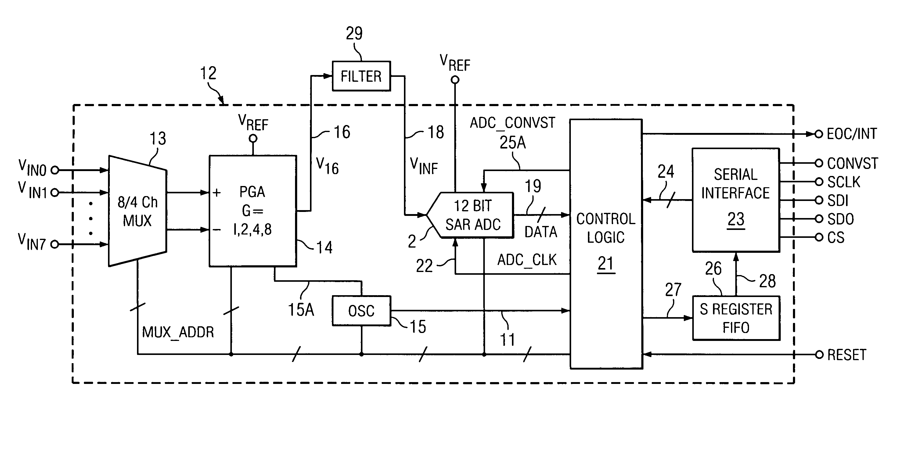
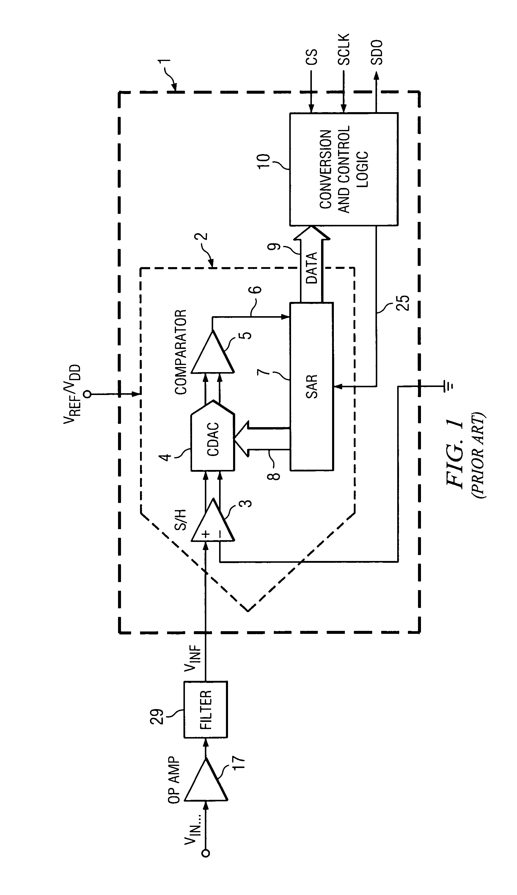
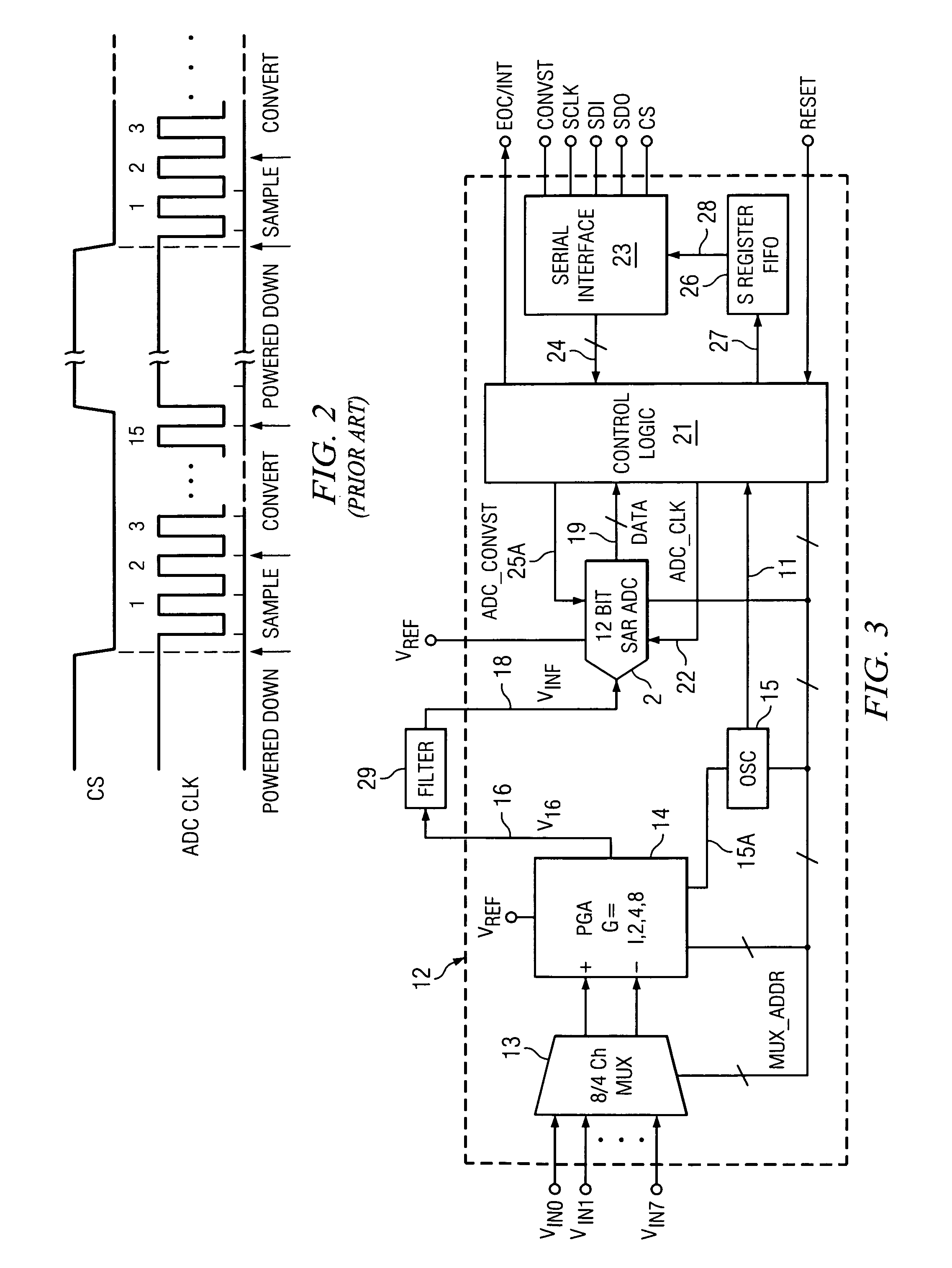
[0031]In FIG. 3, data acquisition system 12 includes a multiplexer 13 that multiplexes a number of analog input signals VIN0,1 . . . 7 to provide the input voltage VIN of a differential programmable gain amplifier (PGA) 14 or other suitable amplifier. PGA 14 produces an amplified output voltage V16 on conductor 16. PGA 14 can be a “continuous time”, chopper stabilized, or switched capacitor sampling amplifier that is clocked in response to a clock signal produced on conductor 15A by an oscillator circuit 15. PGA output voltage V16 can be coupled to the input of an external filter 29, the output signal VINF of which is coupled to the input 18 of a SAR ADC system 2 (which can be similar to SAR ADC 2 of Prior Art FIG. 1). SAR ADC system 2 may be a 12-bit ADC. SAR ADC system 2 is referenced to ground, and receives a reference voltage VREF. SAR ADC system 2 is clocked by a signal ADC_CLK on conductor 22. Multiplexer 13 multiplexes analog input channels specified by a multiplexer address ...


PUM


Abstract

In a data acquisition system, digitizing circuitry (2A) is powered up by a control signal (ADC_CONVST), superimposing a glitch (42-1) on a first multiplexed and amplified signal value (VINF) received by the digitizing circuitry. Sampling and holding of the first multiplexed and amplified signal value occurs during a delay provided between the glitch and a beginning of a first A / D conversion of the first multiplexed and amplified signal value to allow settling of the glitch. After the first conversion begins, a second multiplexed and amplified signal value is generated. The digitizing circuitry performs the first A / D conversion during initial settling of the second multiplexed and amplified signal value and then is powered down while the second multiplexed and amplified signal value continues to settle.

Description

BACKGROUND OF THE INVENTION[0001]The present invention relates generally to low power, relatively high speed (e.g., with sample rates of roughly 100 kilosamples per second (KSPS)) data acquisition circuitry, especially to multi-channel data acquisition circuitry that includes SAR (successive approximation register) ADCs (analog to digital converters).[0002]FIG. 1 shows a SAR ADC conversion circuit 1 which is included in the assignee's commercially available ADS 7866 data acquisition product. SAR ADC conversion circuit 1 receives the amplified output voltage produced by an input amplifier 17. The output of input amplifier 17 can be filtered by an external RC filter 29. Input amplifier 17 receives and amplifies the filtered analog input signal VIN that ultimately is to be digitized. SAR ADC conversion circuit 1 includes a low-power SAR ADC 2 and a conversion and control logic circuit 10.[0003]SAR ADC 2 includes a sample / hold circuit 3 having a (+) input connected to receive the filter...

Claims


Application Information

Patent Timeline
Patent Type & Authority Patents(United States)
IPC IPC(8): H04J3/02
CPCH03M1/0872H03M1/1225H03M1/468
Inventor MOLINA, JOHNNIE F.CHEUNG, HUGO
Owner TEXAS INSTR INC
Why Eureka
Try Eureka