Oxide semiconductor device

a semiconductor and oxide technology, applied in solid-state devices, electric lighting sources, electric light sources, etc., can solve the problems of increased power consumption or leakage current flow, delay in transmission of signals, and distortion of signal waveforms, so as to reduce parasitic capacitance and short channel length , the effect of easy breakag

Active Publication Date: 2013-04-16
SEMICON ENERGY LAB CO LTD
View PDF184 Cites 9 Cited by
  • Summary
  • Abstract
  • Description
  • Claims
  • Application Information

AI Technical Summary

Benefits of technology

[0009]An object of an embodiment of the present invention is to provide a semiconductor device having a structure which enables sufficient reduction in parasitic capacitance.
[0041]By employing the above structure, a semiconductor device with sufficiently reduced parasitic capacitance and a short channel length which is capable of high-speed operation can be provided.

Problems solved by technology

This capacitance is referred to as parasitic capacitance and may cause distortion of signal waveforms.
In addition, when the parasitic capacitance is large, delay of transmission of a signal may be caused.
In addition, an increase in parasitic capacitance will lead to an increase in power consumption or an increase in leakage current which flows when the thin film transistor is OFF.

Method used


Image

  • Oxide semiconductor device
  • Oxide semiconductor device
  • Oxide semiconductor device

Examples


embodiment 1

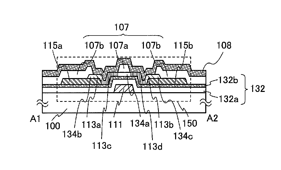
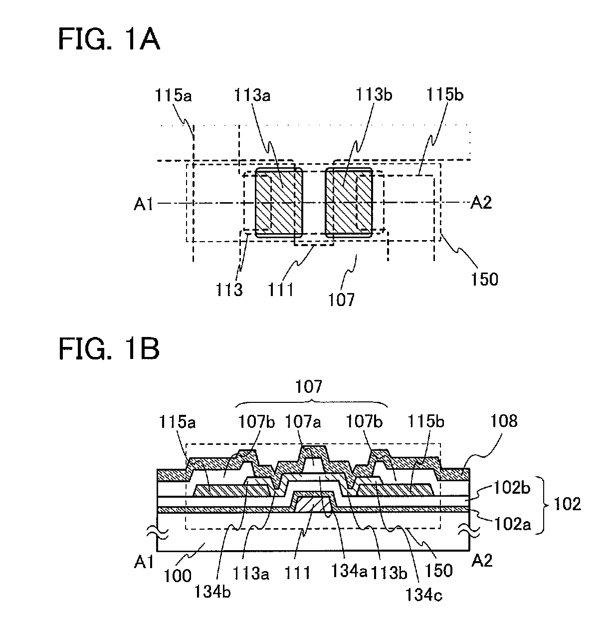
[0078]In this embodiment, an example of a structure of a semiconductor device will be described with reference to FIGS. 1A and 1B. FIG. 1A is a plan view of a thin film transistor 150. FIG. 1B is a cross-sectional view taken along line A1-A2 in FIG. 1A. The thin film transistor 150 has a kind of bottom-gate structure, which is also called a bottom contact (or inverted coplanar) structure.

[0079]As in FIGS. 1A and 1B, the thin film transistor 150 includes a gate electrode layer 111 over a substrate 100 with an insulating surface, a gate insulating layer 102 over the gate electrode layer 111, a source electrode layer 115a and a drain electrode layer 115b over the gate insulating layer 102, an oxide semiconductor layer 113 over the gate insulating layer 102 and the gate electrode layer 111, an oxide insulating layer 107 over the oxide semiconductor layer 113, and a protective insulating layer 108 over the oxide insulating layer 107 and the oxide semiconductor layer 113. Here, the source...

embodiment 2

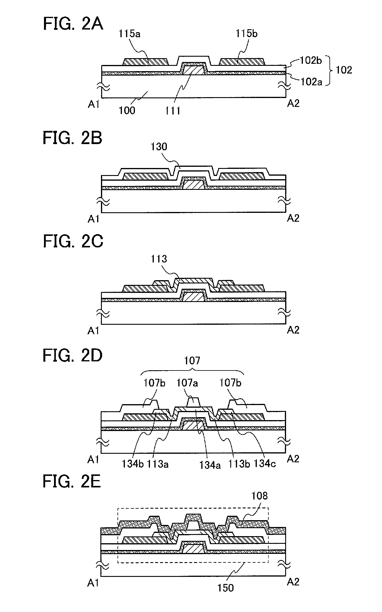
[0109]A mode of a manufacturing method for the semiconductor device described in Embodiment 1 will be described with reference to FIGS. 2A to 2E.

[0110]First, a conductive film or metal conductive film which transmits visible light is formed over the substrate 100 having an insulating surface, and then a first photolithography step is performed to form the gate electrode layer 111. Note that a resist mask may be formed by an ink jetting method. Formation of the resist mask by an ink jetting method needs no photomask; thus, manufacturing cost can be reduced.

[0111]Although there is no particular limitation on a substrate which can be used as the substrate 100 having an insulating surface, it is necessary that the substrate have at least enough heat resistance to withstand heat treatment performed later. For example, a glass substrate can be used as the substrate 100 having an insulating surface.

[0112]As a glass substrate, if the temperature of the heat treatment to be performed later i...

embodiment 3

[0146]In this embodiment, a description will be provided of an example in which an active matrix liquid crystal display device is manufactured by using the thin film transistor described in Embodiment 1 to form a pixel portion and a driver circuit over one substrate.

[0147]FIG. 3 illustrates an example of a cross-sectional structure of the active matrix substrate.

[0148]In this embodiment, a thin film transistor in a pixel portion, a thin film transistor in a driver circuit, a storage capacitor, a gate wiring, a terminal portion of source wiring are described with reference to FIG. 3. The capacitor, the gate wiring, and the terminal portion of the source wiring can be formed in the same manufacturing steps as in Embodiment 2, up to the step of the formation of a protective insulating layer 203 and can be manufactured without an increase in the number of photomasks and an increase in the number of steps. Further, in a portion serving as a display region in the pixel portion, all the ga...


PUM


Abstract

A semiconductor device having a structure which enables sufficient reduction in parasitic capacitance is provided. In addition, the operation speed of thin film transistors in a driver circuit is improved. In a bottom-gate thin film transistor in which an oxide insulating layer is in contact with a channel formation region in an oxide semiconductor layer, a source electrode layer and a drain electrode layer are formed in such a manner that they do not overlap with a gate electrode layer. Thus, the distance between the gate electrode layer and the source electrode layer and between the gate electrode layer and the drain electrode layer are increased; accordingly, parasitic capacitance can be reduced.

Description

TECHNICAL FIELD[0001]The present invention relates to a semiconductor device using an oxide semiconductor and a manufacturing method thereof.[0002]Note that the semiconductor device in this specification refers to all the devices which can operate by using semiconductor characteristics, and an electro-optical device, a semiconductor circuit, and an electronic device are all semiconductor devices.BACKGROUND ART[0003]In recent years, a technique for forming a thin film transistor (TFT) by using a semiconductor thin film (having a thickness of approximately several nanometers to several hundred nanometers) formed over a substrate having an insulating surface has attracted attention. Thin film transistors are applied to a wide variety of electronic devices such as ICs or electro-optical devices, and their development especially as switching elements for an image display device has been accelerated. Various metal oxides are used for a variety of applications. Indium oxide is a well-known...

Claims


Application Information

Patent Timeline
Patent Type & Authority Patents(United States)
IPC IPC(8): H01L29/12H05B44/00
CPCH01L27/1225H01L29/78696H01L29/7869
Inventor YAMAZAKI, SHUNPEITSUBUKU, MASASHIAKIMOTO, KENGOHOSOBA, MIYUKISAKATA, JUNICHIRO
Owner SEMICON ENERGY LAB CO LTD
Why Eureka
Try Eureka