Load-line adaptation

a load-line adaptation and load-line technology, applied in the field of load-line adaptation, can solve the problems of increasing the insertion loss of single l-network, and reducing the insertion efficiency of power amplifiers. the effect of saving energy

Inactive Publication Date: 2013-05-07
QUALCOMM TECHNOLOGIES INC
View PDF20 Cites 12 Cited by
  • Summary
  • Abstract
  • Description
  • Claims
  • Application Information

AI Technical Summary

Benefits of technology

[0008]In one aspect, the present invention provides an adaptive load-line matching network to adapt load impedance over a wide impedance range in accordance with output power levels. Thus, energy could be saved when power amplifiers are operated at medium output power levels.
[0012]In one embodiment the first and second variable circuit elements are variable capacitors. A variable capacitor can be implemented as an array of switchable parallel-connected capacitors. Such switchable capacitors can be realized in MEMS technology, which comprises so-called Micro-electromechanical systems (MEMS). MEMs comprise a collection of micro-sensors and actuators, such as micro switches, micro capacitors and micro inductors and so forth. The integration of MEMS into Radio Frequency (RF) circuits results in systems with superior performance levels and lower manufacturing costs. The incorporation of MEMS based fabrication technologies into micro and millimeter wave systems offers viable routes to ICs with MEMS actuators, antennas, switches and transmission lines. The resultant systems operate with an increased bandwidth and increased radiation efficiency and have considerable scope for implementation within the expanding area of wireless personal communication devices.
[0013]In a further development of the embodiment, the first variable circuit element may further comprise a variable inductor. In order to provide variability, the variable inductor may comprise, similar to the implantation of the variable capacitor, an array of switchable parallel or series connected inductors. By a series circuit of a variable inductor and the variable or fixed capacitor a variable inductor can effectively be realized, which does not require a relative high fixed inductance value. By implementation of the variable series element in the variable impedance switching network with switched inductors (or coils) and variable capacitors, a variable inductor can be attained with a high Q-factor. Thereby the trade-off between tuning range and associated insertion losses can be improved. Again, such a switchable inductor can be made controllable, similar to the variable capacitor, in MEMS technology. A respective applied control setting can be used which corresponds to a digital code stored in a corresponding “inductor”-register, the output of which “inductor”-register is connected to the implemented switched inductors such that the variable inductor is controllable by the digital code stored in the inductor register.
[0028]To sum it up, the general idea lies in the perception of using a fixed matching network between the power transistor and the adaptive matching network, wherein a basic property of the fixed network is to invert, alike a quarter wave transmission line, real load impedances without introducing a significant amount of reactive impedance. The use of such an impedance inverter results in a relatively low insertion loss at high power. In addition, the usage of a fixed matching network allows for the implementation of transmission zeros, for instance to reject harmonics, and / or to provide a well defined load impedance to the power amplifier at a second harmonic, for instance, to obtain inverse class-F operation, independent of the (variable) load impedance at the fundamental frequency.

Problems solved by technology

Commonly, power amplifiers (PA) suffer from low power efficiency at medium output power, because their load-line is typically optimized for maximum output power.
According to theory and simulations, a single L-network gives excessive insertion loss for large impedance transformation ratios.
Moreover, network analysis reveals that the implementation of a variable inductor as a combination of a fixed inductor and variable capacitor makes insertion losses even worse.
This is very undesirable, because it results in a huge PA efficiency degradation at high output power, for which a large impedance transformation ratio is typically required.
Most power amplifiers suffer from low efficiency at medium output power levels, because their load-line is optimized for maximum output power.
Further, for a given quality factor Q of the circuit elements, network insertion losses increase for increasing impedance transformation ratio.
Consequently, losses of a variable matching network tend to become largest at maximum output power.

Method used


Image

  • Load-line adaptation
  • Load-line adaptation
  • Load-line adaptation

Examples


Embodiment Construction

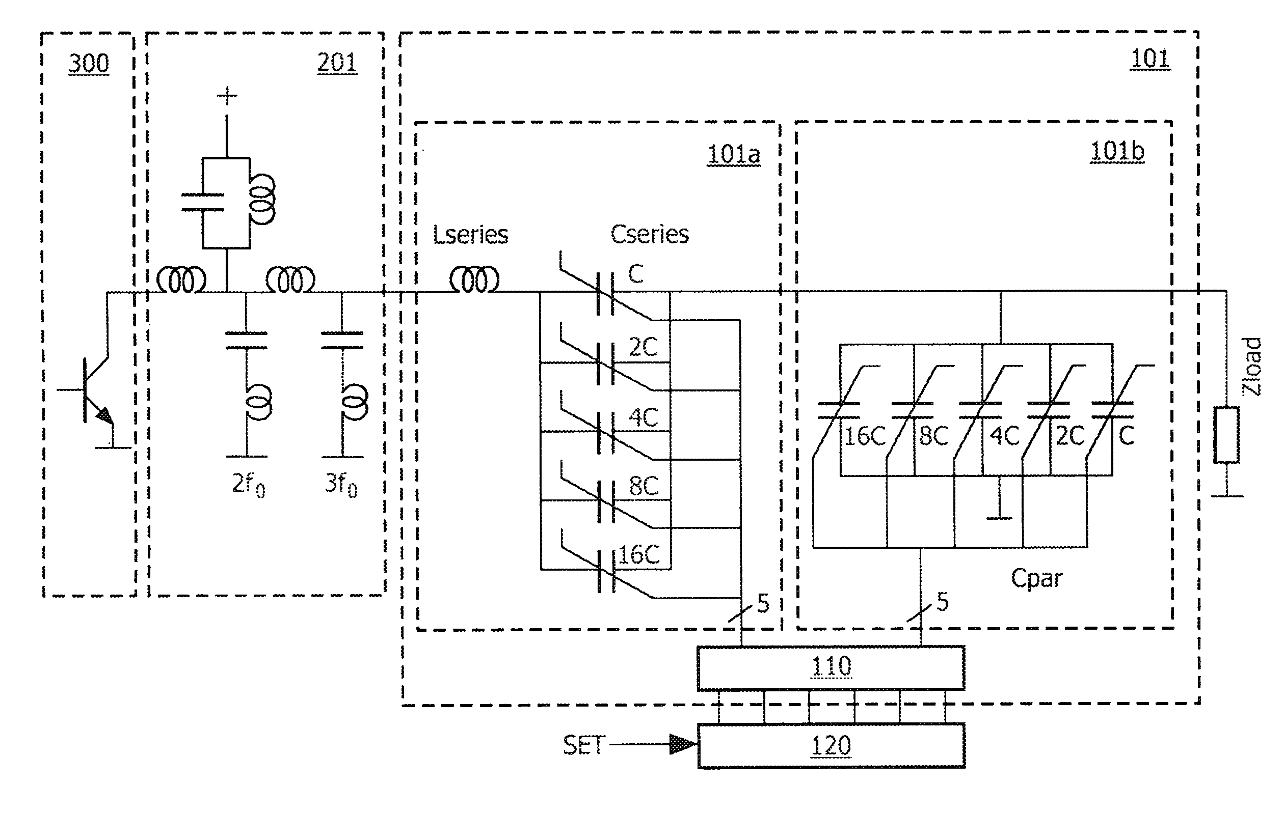
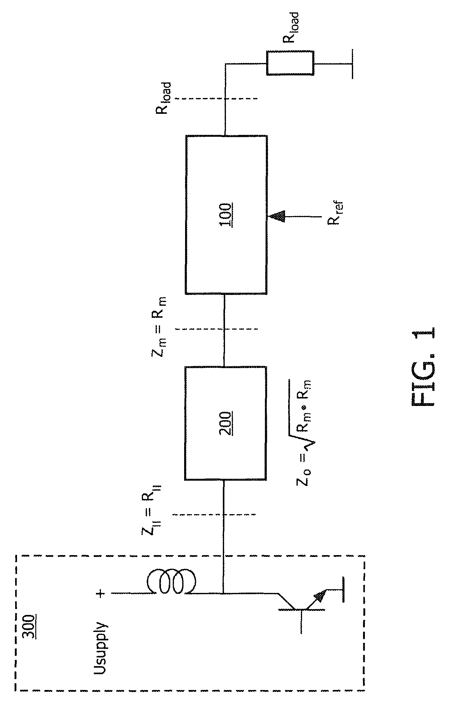
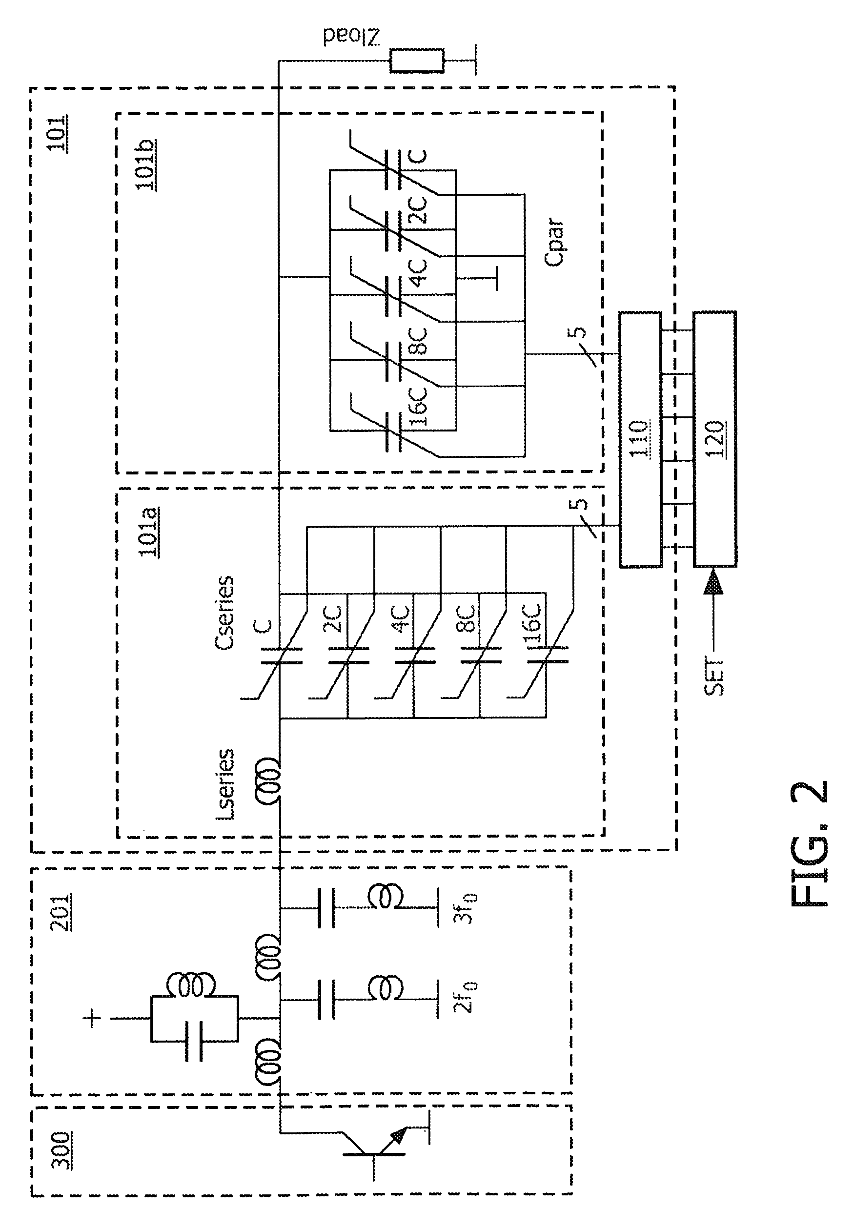
[0039]FIG. 1 shows the general concept of the adaptive load-line matching network as proposed herein is shown. First, a variable matching network 100 transforms a load impedance Rload to a matched impedance Rm, wherein the matching may be arranged such that the matched impedance Rm equals a reference value Rref. Then, a fixed impedance-inverting network 200 having a characteristic impedance of Z0 transforms the matched impedance Rm to a load-line impedance Rll, which is connected to the output of the power amplifier 300 symbolized by a transistor connected to Usupply.

[0040]Optimum efficiency can be obtained by setting the adaptive matching network 100 such that the matched impedance Rm equals Rref as a function of the actual output power of the power amplifier according to the following equation:

[0041]Rm=Rref=Z02·2·Pload(USupply-Usat)2.(0)

[0042]Thus, by the a priori knowledge on the required output power Pload, the supply voltage Usupply, the collector saturation voltage USAT of the...


PUM


Abstract

According to the general concept disclosed herein, a circuit for adaptive matching of a load impedance to a predetermined load-line impedance of a load-line connected to a power amplifier output includes a fixed matching network between the power transistor and an adaptive matching network, whereby the fixed matching network acts as an impedance inverter which results in a relatively low insertion loss at high power. Results indicate that the impedance-inverting network can be used over more than a factor of 10 in impedance variation. Further, the usage of the fixed matching network, close to the power transistor, allows for the implementation of transmission zeros and / or for a well defined load impedance at a predetermined harmonic frequency, independent of the (variable) load impedance at the fundamental frequency.

Description

[0001]This application is a continuation of International Application No. PCT / IB2007 / 052697, filed Jul. 9, 2007, which designated the United States and was published in English, and which claims priority to European Application No. 06117014.8 filed Jul. 12, 2006, both of which applications are incorporated herein by reference.FIELD OF THE INVENTION[0002]The present invention relates to a circuit for adaptive matching of a load impedance to a predetermined load-line impedance of a load-line connected to a power amplifier output, and to a method of adaptive matching of a load impedance to a predetermined load-line impedance at a power amplifier output.BACKGROUND[0003]Commonly, power amplifiers (PA) suffer from low power efficiency at medium output power, because their load-line is typically optimized for maximum output power. Concepts of load-line switching and load-line adaptation are known. For instance, PIN-diode switched capacitors have been implemented in a BGY270 power amplifier...

Claims


Application Information

Patent Timeline
Patent Type & Authority Patents(United States)
IPC IPC(8): H01P5/08H03H7/38
CPCH03F1/56H03F3/191H03H21/0001H03H7/40H03F2200/387H03F2200/451H03F2200/471H03F2200/391H03H21/00H04B1/0458
Inventor VAN BEZOOIJEN, ADRIANUS
Owner QUALCOMM TECHNOLOGIES INC
Why Eureka
Try Eureka