
LED light source, its manufacturing method, and LED-based photolithography apparatus and method

a technology of led light source and manufacturing method, which is applied in the direction of photomechanical equipment, instruments, printers, etc., can solve the problems of shortening the mechanical life of led light source, reducing light intensity, and light intensity, so as to reduce temperature variations, reduce temperature variations, and efficiently transfer

Inactive Publication Date: 2013-05-14
HITACHI HIGH-TECH CORP
View PDF11 Cites 2 Cited by
  • Summary
  • Abstract
  • Description
  • Claims
  • Application Information

AI Technical Summary

Benefits of technology

The LED light source described in the patent text can help reduce temperature variations among LED chips, which can lead to decreased light intensity and shortened LED life. By controlling the temperature, the LED chip can maintain its performance and longevity. Additionally, the LED light source can save power consumption during light exposure in a photolithography apparatus.

Problems solved by technology

When the LED chip is constantly subjected to a high-temperature environment, the LED chip will deteriorate faster, shortening its mechanical life.
For these reasons, increased temperature variations among LED chips lead to adverse consequences such as light intensity decreases, light intensity variations, and shortened LED life.

Method used


Image

  • LED light source, its manufacturing method, and LED-based photolithography apparatus and method
  • LED light source, its manufacturing method, and LED-based photolithography apparatus and method
  • LED light source, its manufacturing method, and LED-based photolithography apparatus and method

Examples


embodiment 1

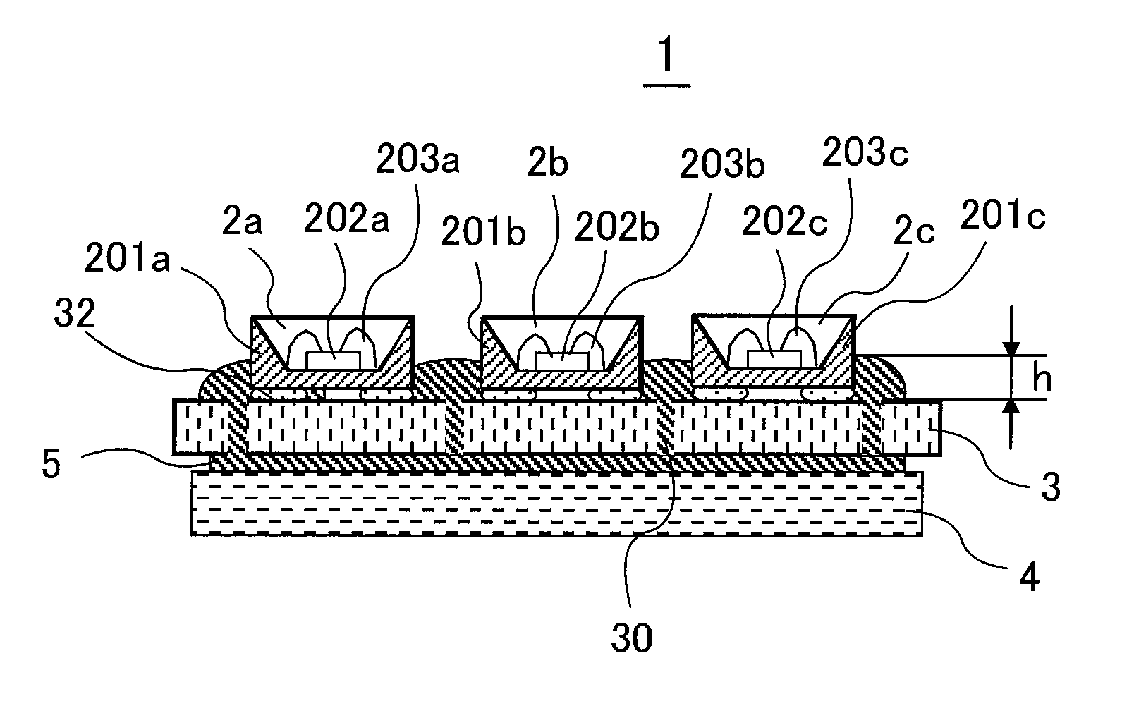
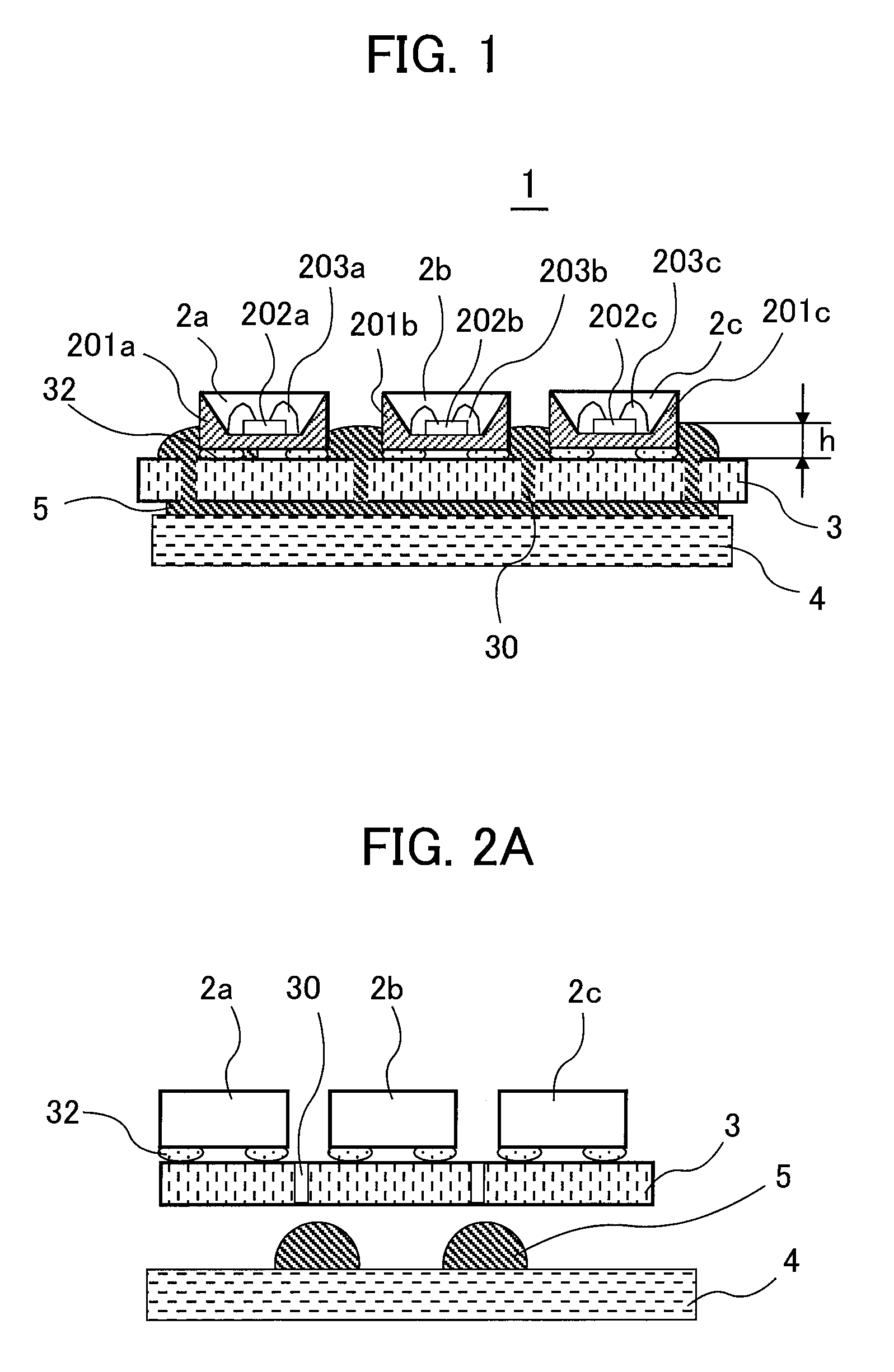
[0042]FIG. 1 is a cross section of an LED light source according to Embodiment 1 of the invention. The LED light source 1 of FIG. 1 includes the following components: a substrate 3; multiple LED substrates 2a to 2c; and a heat sink plate 4. The LED substrates 2a to 2c, that is, substrates on which to mount LEDs, are arranged on the substrate 3 at particular intervals in the form of a single row or multiple rows. The heat sink plate 4 is attached to the bottom surface of the substrate 3. The connection among the LED substrates 2a to 2c, the substrates 3, and the heat sink plate 4 is made by thermally conductive resin 5 (e.g., silicone adhesive).

[0043]Each of the LED substrates 2a to 2c is structurally the same as the LED substrate 10 of FIG. 5. The LED substrates 2a to 2c each include a ceramic substrate 201, an LED chip 202, and wires 203. The ceramic substrate 201 has a square shape with the size of from 2 by 2 mm to 7 by 7 mm and with the thickness of 1.5 to 3 mm. The LED chip 202...

embodiment 2

[0059]FIG. 3 is a cross section of an LED light source according to Embodiment 2 of the invention. As illustrated, protrusions 307 are formed on the top surface of a heat sink plate 304, and alignment holes 308 are formed in a substrate 303 so that each of the protrusions 307 can be inserted into one of the alignment holes 308. By aligning the protrusions 307 with the alignment holes 308, the position of the heat sink plate 304 relative to the substrate 303 can be determined.

[0060]The height of each of the protrusions 307 is greater than the thickness of the substrate 303. Thus, the top ends 307a of the protrusions 307 protrude from the top surface of the substrate 303 on which ceramic substrates 301a and 301b (i.e., LED substrates 300a and 300b) are mounted.

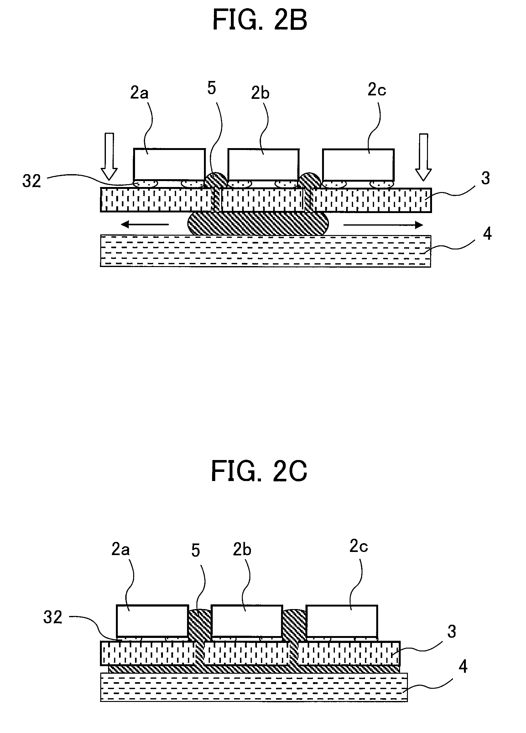
[0061]By applying the same bonding process as illustrated in FIGS. 2A to 2C, thermally conductive resin 305 applied between the heat sink plate 304 and the substrate 303 flows upward from the through holes 309 of the substrate 3...

embodiment 3

[0063]FIG. 4 is a cross section of an LED light source according to Embodiment 3 of the invention, which light source is intended for use in a photolithography apparatus. The LED light source 1A of FIG. 4 differs from its counterparts of Embodiments 1 and 2 in that a lens substrate 402 is placed on the ceramic substrates 401 of LED substrates 410. The lens substrate 402 has windows 411, and a lens 412 is fit in each of the windows 411 in order to prevent light dispersion. Each of the lenses 412 is designed to convert radial light rays emitted from the LED substrates 410 into parallel ones.

[0064]Each of the lenses 412 has a transmittance of 50% or greater at the wavelength of the light from the LED substrates 410 and is molded from inorganic glass such as quartz or the like or from organic resin such as silicone resin, acrylic resin, or epoxy resin. The lenses 412 can be spherical lenses, aspherical lenses, or Fresnel lenses.

[0065]The LED light source 1A of FIG. 4 can be fabricated b...


PUM


Abstract

This invention provides a structurally-simple LED light source that is capable of preventing temperature variations among its multiple LED elements arranged densely on its LED-mounting substrate and also improving the heat release capabilities of the substrate by comprising an LED light source with: a plurality of LED elements each of which is formed by connecting an LED chip to electrodes formed on a ceramic substrate; an LED-mounting substrate on which to mount the plurality of LED elements, the LED-mounting substrate having through holes therein; and a heat sink plate for releasing heat from the LED-mounting substrate, wherein a thermally conductive resin is present between the LED-mounting substrate and the heat sink plate and wherein part of the thermally conductive resin protrudes from the through holes of the LED-mounting substrate and covers the top surface of the LED-mounting substrate on which the plurality of LED elements are mounted, so that the part of the thermally conductive resin is in contact with the plurality of LED elements.

Description

CROSS-REFERENCE TO RELATED PATENT APPLICATIONS[0001]Priority is claimed to Japan Priority Application 2009-155179, filed Jun. 30, 2009 including the specification, drawings, claims and abstract which are incorporated herein by reference in their entirety.BACKGROUND OF THE INVENTION[0002]As an example of a conventional LED (light-emitting diode) substrate, Japanese Unexamined Patent Application Publication No. 2004-311791 (Patent Document 1) discloses such an LED substrate as illustrated in FIG. 5.[0003]The LED substrate 10 of FIG. 5 has a concave portion 11a formed on the top surface of its ceramic substrate 11. Conductive wiring patterns 12 are formed on the concave portion 11a, and a single LED chip 13 is glued to the conductive wiring patterns 12 with its bottom surface facing the concave portion 11a (the bottom surface of the LED chip 13 is the surface through which light is not emitted). The electrodes on the light-emitting-surface side of the LED chip 13 are connected by wires...

Claims


Application Information

Patent Timeline
Patent Type & Authority Patents(United States)
IPC IPC(8): G03B27/54H01L21/00H01L33/00
CPCG03F7/7005H01L33/64H05B3/0038H05K1/0204H05K3/0061G03F7/70858H01L25/13H01L33/641H01L2224/48091H05K1/0206H05K2201/0209H05K2201/09063H05K2201/10106H05K2201/10977H01L2924/00014G03F7/2004H01L21/0275
Inventor ISHIDA, SUSUMUHATA, SHOHEI
Owner HITACHI HIGH-TECH CORP
Learn More