Low temperature silicon oxide conversion

a technology of silicon oxide and conversion temperature, applied in the field of low temperature silicon oxide conversion, can solve the problems of dielectric material, dielectric material, and reduced structural features of the device, and achieve the effect of reducing the spatial dimension of the device, and reducing the cost of dielectric material

Active Publication Date: 2013-05-21
APPLIED MATERIALS INC
View PDF416 Cites 18 Cited by
  • Summary
  • Abstract
  • Description
  • Claims
  • Application Information

AI Technical Summary

Problems solved by technology

The decreasing feature sizes result in structural features on the device having decreased spatial dimensions.
The widths of gaps and trenches on the device narrow to a point where the aspect ratio of gap depth to its width becomes high enough to make it challenging to fill the gap with dielectric material.
The depositing dielectric material is prone to clog at the top before the gap completely fills, producing a void or seam in the middle of the gap.
However, once these highly flowable materials are deposited, they have to be hardened into a solid dielectric material.
Unfortunately, the departing carbon and hydroxyl species often leave behind pores in the hardened dielectric that reduce the quality of the final material.
In addition, the hardening dielectric also tends to shrink in volume, which can leave cracks and spaces at the interface of the dielectric and the surrounding substrate.
High temperature exposure to oxygen environments can ruin underlying films for some circuit architectures.
This consideration results in the need to stay within a “thermal budget” during a manufacturing process flow.
Thermal budget considerations have largely limited SOD to process flows incorporating an underlying silicon nitride layer which can protect underlying features from oxidation (e.g. DRAM applications).

Method used


Image

  • Low temperature silicon oxide conversion
  • Low temperature silicon oxide conversion
  • Low temperature silicon oxide conversion

Examples


Embodiment Construction

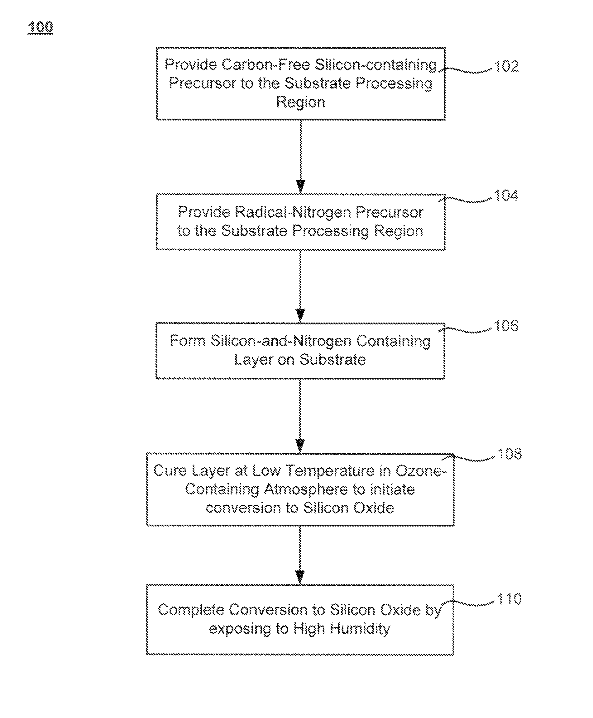
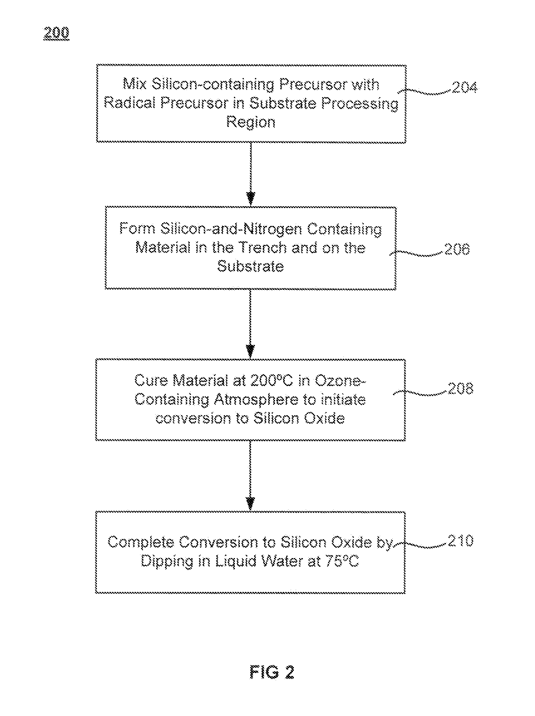
[0017]A method of forming a silicon oxide layer is described. The method first deposits a silicon-nitrogen-and-hydrogen-containing (polysilazane) film by radical-component chemical vapor deposition (CVD). The polysilazane film is converted to silicon oxide by exposing the polysilazane film to humidity at low substrate temperature. The polysilazane film may also be dipped in a liquid having both oxygen and hydrogen, such as water, hydrogen peroxide and or ammonium hydroxide. These conversion techniques may be used separately or in a sequential combination. Conversion techniques described herein hasten conversion, produce manufacturing-worthy films and remove the requirement of a high temperature oxidation treatment. An ozone treatment may precede the conversion technique(s).

[0018]Exposing a radical-component CVD silicon-nitrogen-and-hydrogen-containing film to a humid atmosphere has been found to accelerate the completion of the transition to silicon oxide as determined by fourier tr...


PUM

PropertyMeasurementUnit
temperatureaaaaaaaaaa

Abstract

A method of forming a silicon oxide layer is described. The method first deposits a silicon-nitrogen-and-hydrogen-containing (polysilazane) film by radical-component chemical vapor deposition (CVD). The polysilazane film is converted to silicon oxide by exposing the polysilazane film to humidity at low substrate temperature. The polysilazane film may also be dipped in a liquid having both oxygen and hydrogen, such as water, hydrogen peroxide and or ammonium hydroxide. These conversion techniques may be used separately or in a sequential combination. Conversion techniques described herein hasten conversion, produce manufacturing-worthy films and remove the requirement of a high temperature oxidation treatment. An ozone treatment may precede the conversion technique(s).

Description

CROSS-REFERENCES TO RELATED APPLICATIONS[0001]This application claims the benefit of U.S. Prov. Pat. App. No. 61 / 477,515 filed Apr. 20, 2011, and titled “LOW TEMPERATURE SILICON OXIDE CONVERSION,” which is incorporated herein by reference for all purposes.BACKGROUND OF THE INVENTION[0002]Semiconductor device geometries have dramatically decreased in size since their introduction several decades ago. Modern semiconductor fabrication equipment routinely produce devices with 45 nm, 32 nm, and 28 nm feature sizes, and new equipment is being developed and implemented to make devices with even smaller geometries. The decreasing feature sizes result in structural features on the device having decreased spatial dimensions. The widths of gaps and trenches on the device narrow to a point where the aspect ratio of gap depth to its width becomes high enough to make it challenging to fill the gap with dielectric material. The depositing dielectric material is prone to clog at the top before the ...

Claims


Application Information

Patent Timeline
Patent Type & Authority Patents(United States)
IPC IPC(8): H05H1/24
CPCC23C16/345C23C16/56H01L21/02271H01L21/02164H01L21/02205H01L21/324
Inventor LIANG, JINGMEIINGLE, NITIN K.HONG, SUKWONPATEL, ANJANA M.
Owner APPLIED MATERIALS INC
Why Eureka
Try Eureka