Sidewall image transfer using the lithographic stack as the mandrel

a technology of lithographic stack and sidewall, applied in the field of photolithography, can solve the problems of power consumption control issues, performance degradation, yield loss, etc., and achieve the effects of reducing the size of structural features, reducing cost and size, and increasing the amount of circuitry

Inactive Publication Date: 2013-06-04
IBM CORP
View PDF30 Cites 24 Cited by
  • Summary
  • Abstract
  • Description
  • Claims
  • Application Information

AI Technical Summary

Benefits of technology

[0003]Photolithography is a technique for transferring an image rendered on one media onto another media photographically. Photolithography techniques are widely used in semiconductor fabrication. Typically, a circuit pattern is rendered as a positive or negative mask image which is then projected onto a silicon substrate coated with photosensitive materials (e.g., PR). Radiation impinges on the masked surface to chemically change those areas of the coating exposed to the radiation, usually by polymerizing the exposed coating. The unpolymerized areas are removed, being more soluble in the developer than the polymerized regions, and the desired image pattern remains.
[0004]Semiconductors and integrated circuit chips have become ubiquitous within many products due to their continually decreasing cost and size. In the microelectronics industry as well as in other industries involving construction of microscopic structures (e.g., micromachines, magnetoresistive heads, etc.) there is a continued desire to reduce the size of structural features and microelectronic devices and / or to provide a greater amount of circuitry for a given chip size. Miniaturization in general allows for increased performance (more processing per clock cycle and less heat generated) at lower power levels and lower cost. Present technology is at or approaching atomic level scaling of certain micro-devices such as logic gates, FETs and capacitors, for example. Circuit chips with hundreds of millions of such devices are not uncommon. Further size reductions appear to be approaching the physical limit of trace lines and micro-devices that are embedded upon and within their semiconductor substrates. The present invention is directed to such micro-sized devices.
[0005]Effective lithographic techniques are essential for achieving reduction of feature sizes. Lithography impacts the manufacture of microscopic structures, not only in terms of directly imaging patterns on the desired substrate, but also in terms of making masks typically used in such imaging. Typical lithographic processes involve formation of a patterned resist layer by patternwise exposing a radiation-sensitive resist to an imaging radiation. The image is subsequently developed by contacting the exposed resist layer with a material (typically an aqueous alkaline developer) to selectively remove portions of the resist layer to reveal the desired pattern. The pattern is subsequently transferred to an underlying material by etching the material in openings of the patterned resist layer. After the transfer is complete, the remaining resist layer is removed.
[0006]For some lithographic imaging processes, the resist used does not provide sufficient resistance to subsequent etching steps to enable effective transfer of the desired pattern to a layer underlying the resist. In many instances (e.g., where an ultrathin resist layer is desired, where the underlying material to be etched is thick, where a substantial etching depth is required and / or where it is desired to use certain etchants for a given underlying material), a so-called HM layer is used intermediate between the resist layer and the underlying material to be patterned by transfer from the patterned resist. The HM layer receives the pattern from the patterned resist layer and should be able to withstand the etching processes needed to transfer the pattern to the underlying material.
[0007]Also, where the underlying material layer is excessively reflective of the imaging radiation used to pattern the resist layer, a thin ARC is typically applied between the underlying layer and the resist layer. In some instances, the ARC and HM functions may be served by a same material. In other cases, an OPL may be used as a softmask. The OPL serves two roles. First, the OPL helps define the depth of focus by ensuring smooth planarization. Second, the OPL acts as an ARC to reduce or prevent reflections of the incident laser beam. Other liquid or viscous films may be utilized instead of an OPL to achieve similar performance. One non-limiting example of an OPL is ODL.
[0008]Basically, a FET is a transistor having a source, a gate, and a drain. The action of the FET depends on the flow of majority carriers along a channel between the source and drain that runs past the gate. Current through the channel, which is between the source and drain, is controlled by the transverse electric field under the gate. More than one gate (multi-gate) can be used to more effectively control the channel. The length of the gate determines how fast the FET switches, and can be about the same as the length of the channel (i.e., the distance between the source and drain). Multi-gate FETs are considered to be promising candidates to scale CMOS FET technology down to the sub-22 nm regime.

Problems solved by technology

Semiconductors and integrated circuit chips have become ubiquitous within many products due to their continually decreasing cost and size.
For some lithographic imaging processes, the resist used does not provide sufficient resistance to subsequent etching steps to enable effective transfer of the desired pattern to a layer underlying the resist.
Also, where the underlying material layer is excessively reflective of the imaging radiation used to pattern the resist layer, a thin ARC is typically applied between the underlying layer and the resist layer.
Similarly, line width control problems during gate electrode definition for small devices can lead to performance degradation, power consumption control issues and yield loss.
However, current state-of-the-art lithographic technology cannot adequately and efficiently satisfy the ever-increasing demand for smaller devices and device components.

Method used


Image

  • Sidewall image transfer using the lithographic stack as the mandrel
  • Sidewall image transfer using the lithographic stack as the mandrel
  • Sidewall image transfer using the lithographic stack as the mandrel

Examples


Embodiment Construction

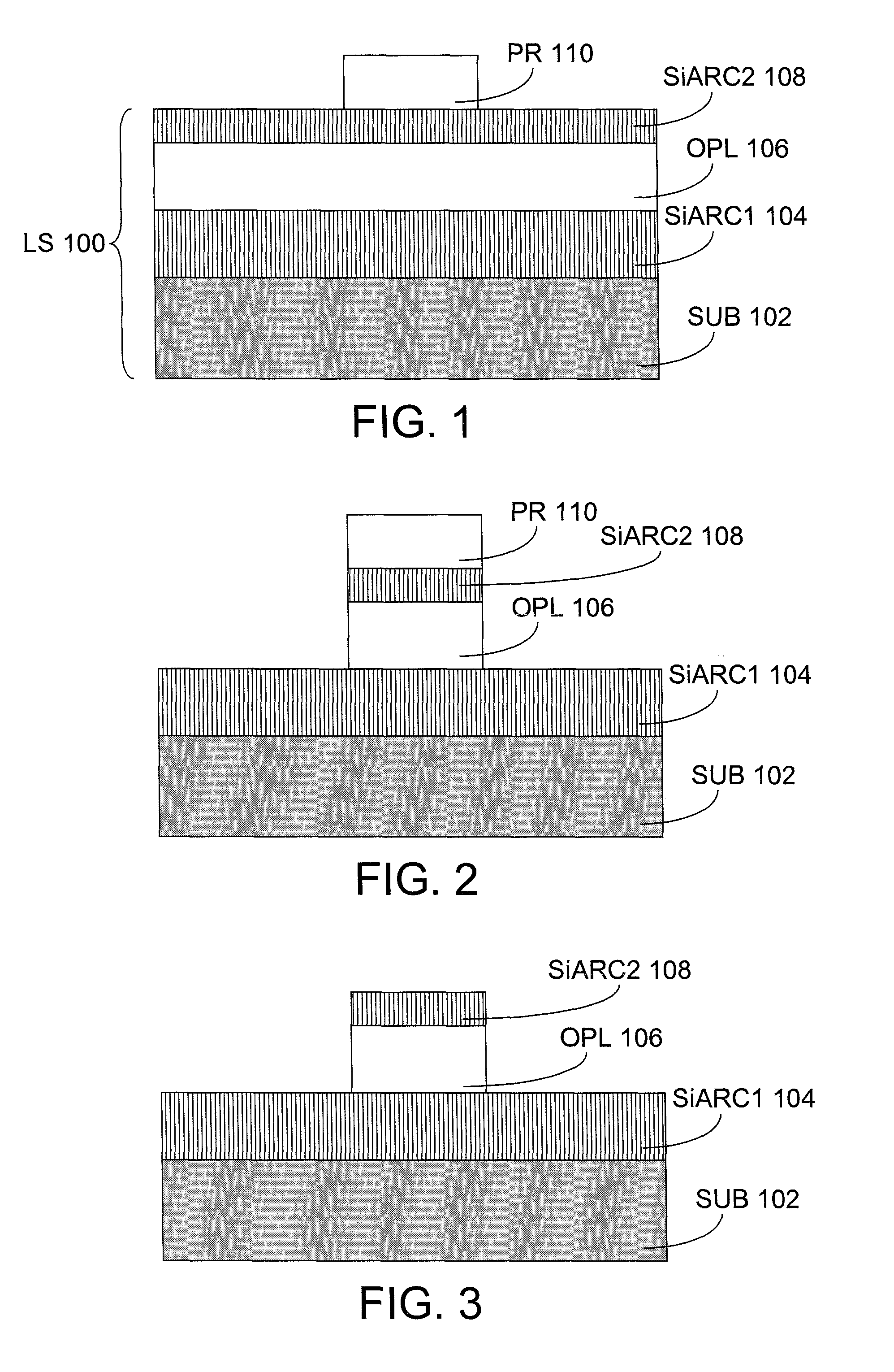
[0025]Pitch doubling (i.e., spatial frequency doubling) will likely become ubiquitous as semiconductor production focuses on smaller sizes (e.g., 22 nm or smaller). What is needed is a lithographic (litho) level agnostic pitch doubling scheme with a low COO. Since the spacer sets the CD, very tight control of conformality and deposition thickness is needed.

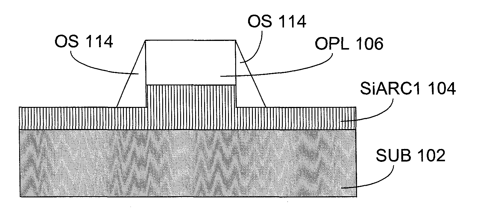
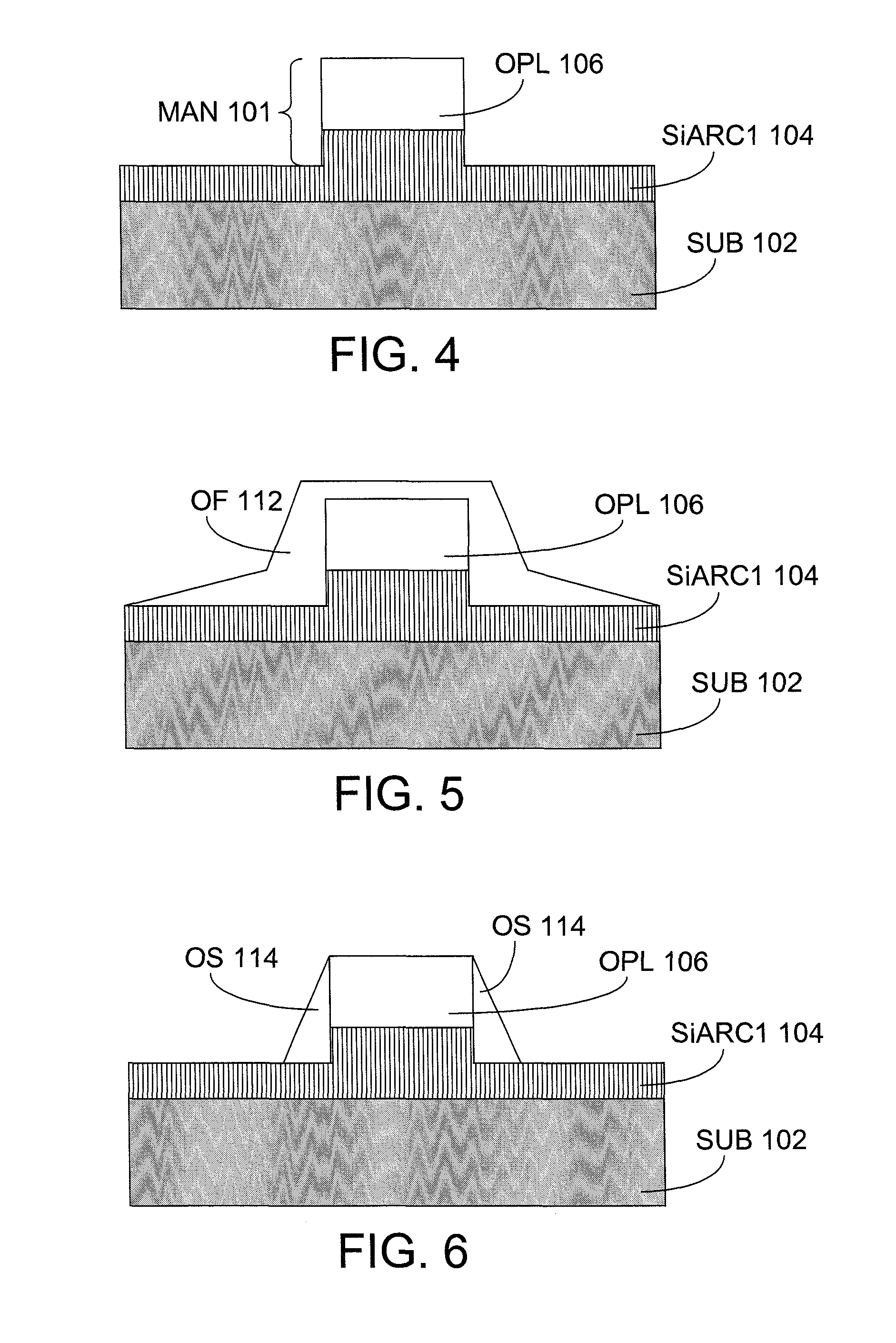
[0026]Current SIT techniques utilize a poly (polycrystalline silicon) mandrel. The SiN spacer is deposited (e.g., using PECVD) around the poly mandrel. The mandrel is removed and the remaining spacer is used as a mask for lower levels (e.g., the spacer image is transferred down to the lower levels). This process tends to necessitate usage of high temperatures for the poly. These high temperatures are not compatible with BEOL levels. In addition, the COO is higher because of the sacrificial mandrel deposition (i.e., deposition of mandrel layers, used for forming the sacrificial mandrel).

[0027]In view of the foregoing, the exemplary...


PUM

PropertyMeasurementUnit
thicknessaaaaaaaaaa
thicknessaaaaaaaaaa
thicknessaaaaaaaaaa

Abstract

In one non-limiting exemplary embodiment, a method includes: providing a structure having at least one lithographic layer on a substrate, where the at least one lithographic layer includes a planarization layer (PL); forming a sacrificial mandrel by patterning at least a portion of the at least one lithographic layer using a photolithographic process, where the sacrificial mandrel includes at least a portion of the PL; and producing at least one microstructure by using the sacrificial mandrel in a sidewall image transfer process.

Description

TECHNICAL FIELD[0001]The exemplary embodiments of this invention relate generally to photolithography and, more specifically, relate to sidewall image transfer techniques and processes and products formed thereby.BACKGROUND[0002]The following abbreviations are utilized herein:ALD atomic layer depositionARC antireflective coatingBEOL back end of lineBoX buried oxideCD critical dimensionCMOS complementary metal-oxide semiconductorCOO cost of ownershipCVD chemical vapor depositionFET field effect transistorHM hardmaskMLD multilayer depositionNFC near frictionless carbonOPL organic planarization layerPC photonic crystalPD pitch doublingPECVD plasma enhanced chemical vapor depositionPR photoresistRIE reactive ion etchSOI silicon-on-insulatorSIT sidewall image transferSTI shallow trench isolation[0003]Photolithography is a technique for transferring an image rendered on one media onto another media photographically. Photolithography techniques are widely used in semiconductor fabrication....

Claims


Application Information

Patent Timeline
Patent Type & Authority Patents(United States)
IPC IPC(8): H01L21/302
CPCH01L21/0337H01L21/0338H01L21/3086H01L21/3088H01L21/32139H01L29/66795
Inventor KANAKASABAPATHY, SIVANANDA K.
Owner IBM CORP
Why Eureka
Try Eureka