Light emitting device

a technology of light-emitting devices and light-emitting devices, which is applied in the direction of semiconductor devices for light sources, point-like light sources, lighting and heating apparatus, etc., can solve the problems of high production cost, only having a 50% payload, and general inconvenient arrangemen

Active Publication Date: 2013-06-11
EPISTAR CORP
View PDF35 Cites 36 Cited by
  • Summary
  • Abstract
  • Description
  • Claims
  • Application Information

AI Technical Summary

Benefits of technology

[0013]To provide environmental protection to the light emitting diodes each recess can be substantially filled with a substantially transparent material, for example a polymer such as a UV or thermally curable silicone or epoxy, to encapsulate each light emitting diode. Advantageously, at least one phosphor material is incorporated in the transparent material, said phosphor material being operable to absorb at least a part of the light emitted by its associated light emitting diode and to re-emit light of a different wavelength.
[0018]To maximize the number of light emitting diodes that can be housed on a given area of substrate, the array of recesses is preferably configured as a square array. In one implementation that is configured for 110V operation the array of recesses comprises a square array of forty nine apertures of which forty five are configured to house a respective light emitting diode and the remaining four can each house a rectifier diode.

Problems solved by technology

Although such a fabrication is compact it has a disadvantage that since only one LED string is energized at a time the arrangement has only a 50% payload.
Whilst such an arrangement can achieve a very high packing density of LEDs per unit area of wafer (of the order of 100 to 400 per square cm (cm2) depending on the size of the LED chip) it has a fundamental drawback in that during fabrication a failure of a single LED means that the entire device has to be discarded resulting in a high production cost.
However, such an arrangement is generally not suited to white LEDs which additionally require a layer of wavelength converting phosphor over the light emitting face of each LED.

Method used


Image

  • Light emitting device
  • Light emitting device
  • Light emitting device

Examples


Embodiment Construction

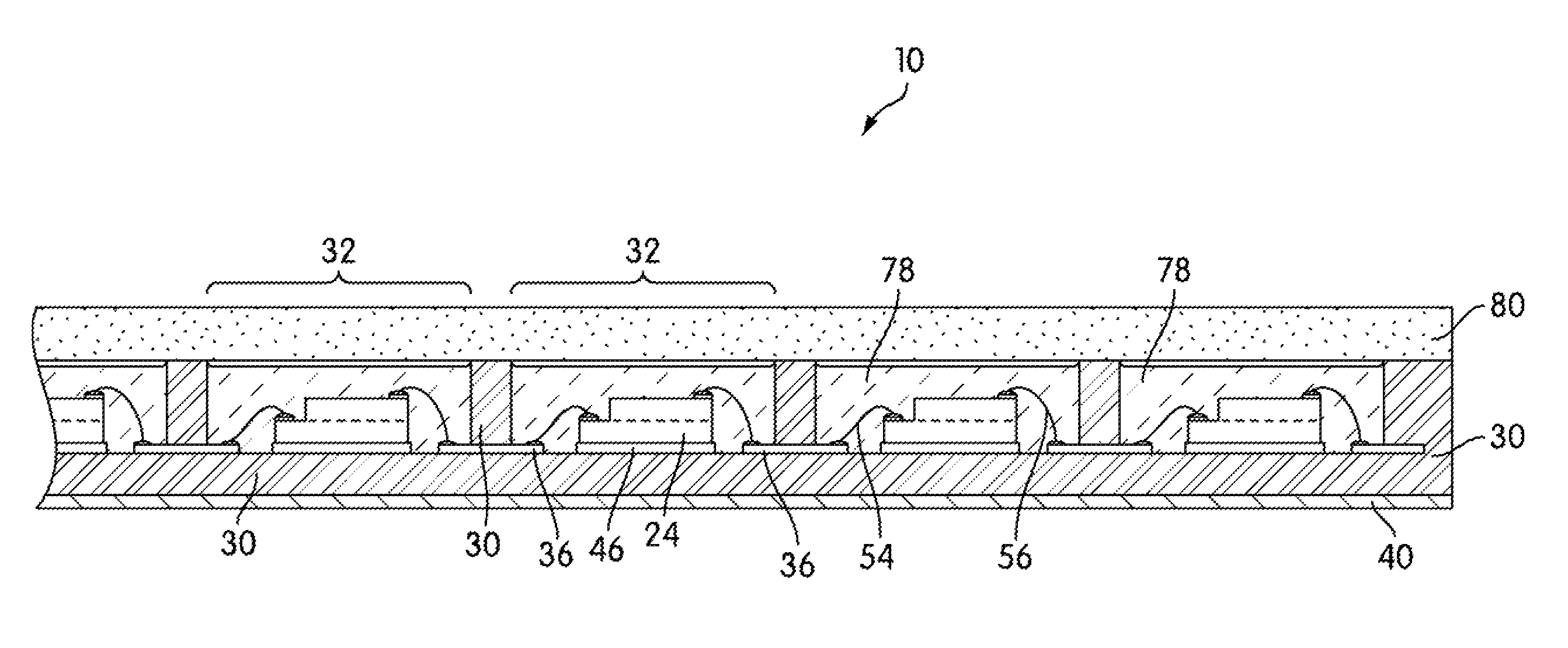
[0035]A white light emitting AC light emitting device 10 in accordance with a first embodiment of the invention will now be described with reference to FIGS. 1 to 5 of the accompanying drawings. The AC light emitting device 10 is configured for direct operation from a 110V (r.m.s.) AC (60 Hz) mains power supply as is found in North America.

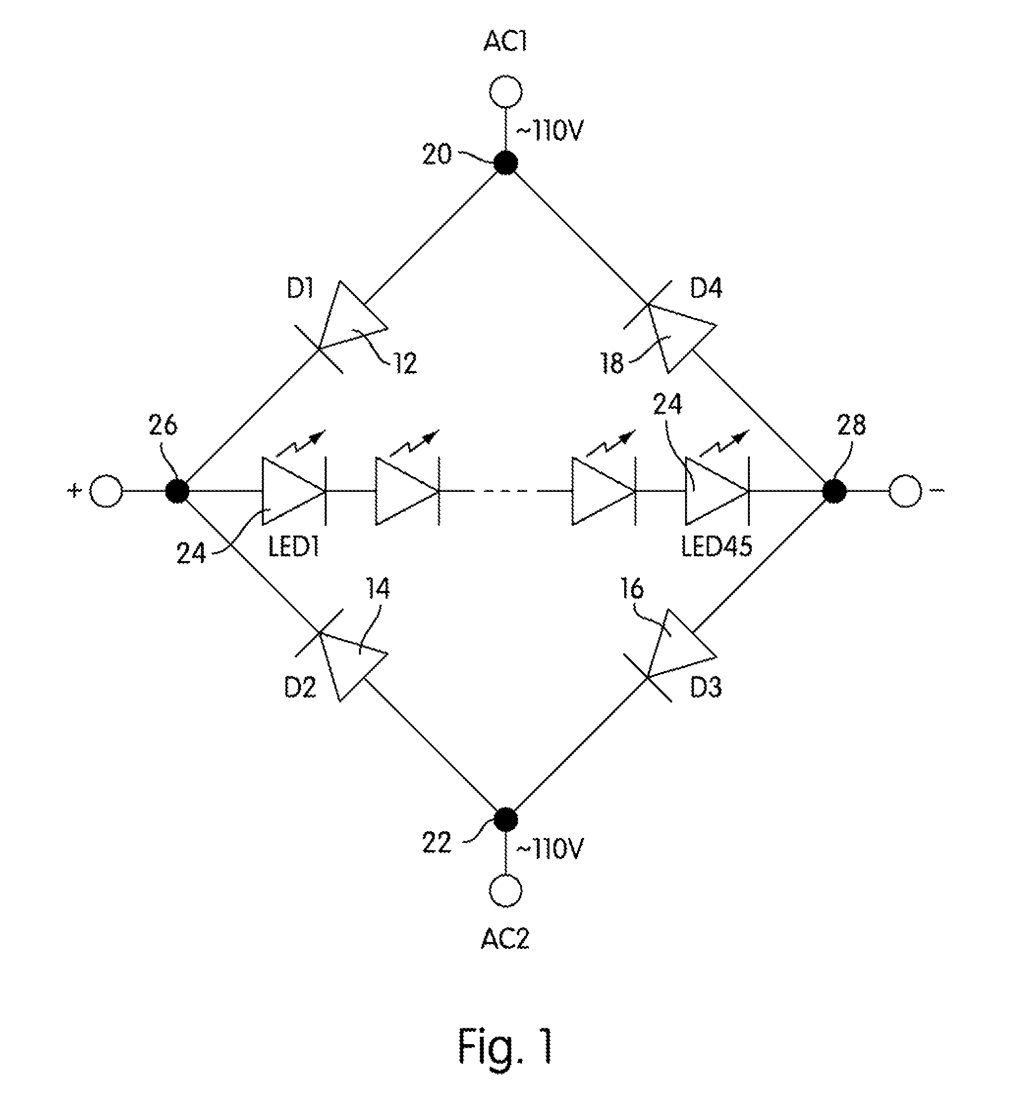
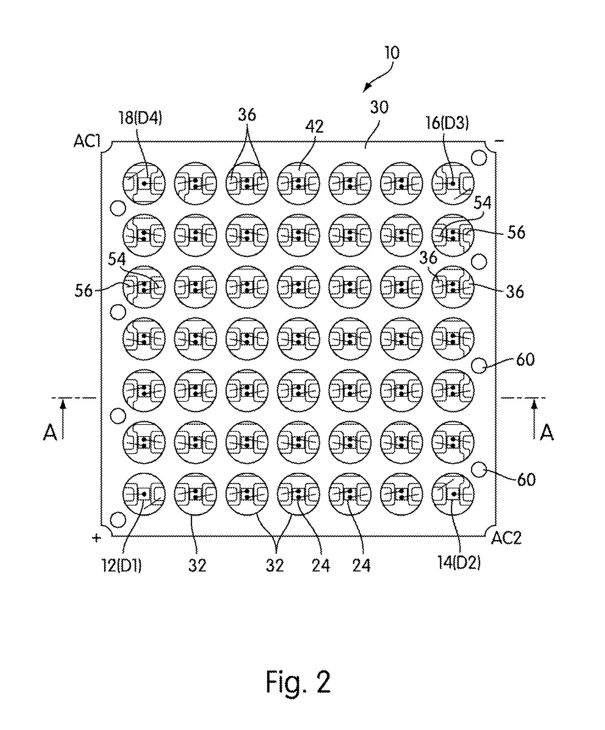
[0036]FIG. 1 is a circuit diagram of the AC light emitting device 10 of the invention and comprises four rectifier diodes 12, 14, 16, 18 (D1 to D4) connected in series in a closed loop bridge configuration. The rectifier diodes (D1 to D4) can comprise silicon, germanium, silicon carbide, or gallium nitride devices. A mains 110V AC power source is connectable to opposite nodes 20 and 22 (AC1 and AC2) of the bridge and forty five series-connected gallium nitride-based blue or UV emitting LED chips 24 (LED1 to LED45) connected between the rectified positive 26 (+) and negative 28 (−) nodes of the diode bridge. For 110V operation each LED chip 24 drop...


PUM


Abstract

A light emitting device comprises: a plurality of light emitting diodes and an insulating (low temperature co-fired ceramic) substrate with an array of recesses each for housing a respective one of the light emitting diodes. The substrate incorporates a pattern of electrical conductors that is configured for connecting the light emitting diodes in a selected electrical configuration and to provide at least two electrical connections on the floor of each recess. Light emitting diodes can be electrically connected to the electrical connections by at least one bond wire or by flip chip bonding. Each recess is filled with a transparent material to encapsulate each light emitting diode. The transparent material can incorporate at least one phosphor material such that the device emits light of a selected color and / or color temperature.

Description

BACKGROUND OF THE INVENTION[0001]1. Field of the Invention[0002]This invention relates to a light emitting device based on a plurality of light emitting diodes (LEDs). In particular, although not exclusively, the invention concerns an alternating current (AC) driven light emitting device that can be operated from a high voltage (110 / 220V) supply. Moreover, the invention concerns AC light sources based on a plurality of such light emitting devices.[0003]2. Description of the Related Art[0004]As is known LEDs are intrinsically direct current (DC) devices that will only pass an electrical current in a single direction and have traditionally been driven by low voltage (e.g. 3.5V for gallium nitride LEDs) DC sources.[0005]White light generating LEDs, “white LEDs”, are a relatively recent innovation and offer the potential for a whole new generation of energy efficient lighting systems to come into existence. It is predicted that white LEDs could replace incandescent, fluorescent and comp...

Claims


Application Information

Patent Timeline
Patent Type & Authority Patents(United States)
IPC IPC(8): H01L25/03
CPCH05B33/12F21K9/30F21Y2101/02H01L25/0753H05K1/0206H05K3/284H01L2224/73265F21Y2103/003H01L2224/48091H01L2224/49107H01L2924/00F21K9/20F21Y2103/10F21Y2115/10H01L2924/00014F21S4/28H01L33/48H01L33/507H01L33/644
Inventor CHOU, HSI-YANSU, HWALI, YI-QUN
Owner EPISTAR CORP
Why Eureka
Try Eureka