Method of depositing film by atomic layer deposition with pulse-time-modulated plasma

a technology of pulse-time modulated plasma and atomic layer, which is applied in the direction of chemical vapor deposition coating, plasma technique, coating, etc., can solve the problems of affecting the the inability to fully complete the deposition process in a long time, and the inability to achieve the effect of reducing the surface potential and significantly improving the in-plane uniformity of the resultant film

Active Publication Date: 2013-06-18
ASM JAPAN
View PDF12 Cites 382 Cited by
  • Summary
  • Abstract
  • Description
  • Claims
  • Application Information

AI Technical Summary

Benefits of technology

[0008]In at least one of the disclosed embodiments of the present invention, surface potential can effectively be controlled at each cycle during atomic layer deposition. In at least one of the disclosure embodiments, in-plane uniformity of a resultant film can significantly be improved. An embodiment of the present invention provides a method of forming a thin film by alternating multiple times, respectively, a process of adsorbing a precursor onto a substrate and a process of treating the adsorbed surface using a reactant gas and a plasma, wherein the reactant gas is supplied substantially uniformly over the substrate, and the plasma is pulse-time-modulated and applied in the process of supplying the reactant gas. In some embodiments, no reactant gas is supplied in the precursor adsorption process. In some embodiments, a purge process is provided between the precursor adsorption process and plasma treatment process using a reactant gas. In some embodiments, the pulse-time-modulated RF power is constituted by a plurality of pulses wherein one cycle of each pulse is about 3 msec to about 1,000 msec (typically about 100 msec to about 500 msec), and a duty of the cycle is about 60% or higher (typically about 75% or higher).

Problems solved by technology

To deposit a thick film, it requires a cyclic deposition of at least several hundred times, taking a long time to complete the deposition process.
In the above, since plasma treatment is repeated at least several hundred times, surface potential on the wafer increases as a result of accumulating floating potential on the wafer, leading to the following risks: wafer slip, wafer sticking on a susceptor, and destruction of gate elect loads in a patterned wafer.
However, the above surface potential problems have not been recognized because PE-ALD predominantly targets a thin film and thus, it is believed that surface potential does not increase significantly on the wafer.
Thus, no solutions to the aforementioned problems have been provided.
However, the present inventor expects that the problems will become more significant in the future because there is a demand for finer, more complex layered structures and patterns, and a combination with other layers and other treatments, wherein surface potential and in-plane uniformity of a film by PE-ALD may affect characteristics of a final product.
However, this technology is not suitable for PE-ALD because PE-ALD is a highly cyclic process, and surface potential accumulates at each cycle.
However, such short pulse-time-modulation is used to alternately emit positive ions and negative ions to a wafer, thereby inhibiting accumulation of electrons and increasing etching speed, and this technology is unrelated to PE-ALD.

Method used


Image

  • Method of depositing film by atomic layer deposition with pulse-time-modulated plasma
  • Method of depositing film by atomic layer deposition with pulse-time-modulated plasma
  • Method of depositing film by atomic layer deposition with pulse-time-modulated plasma

Examples


example 1

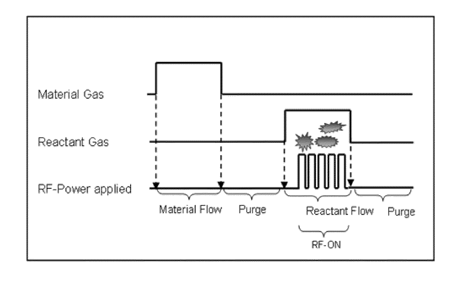
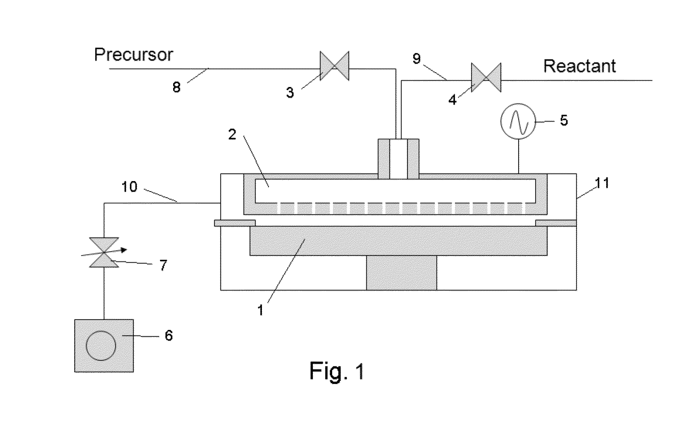
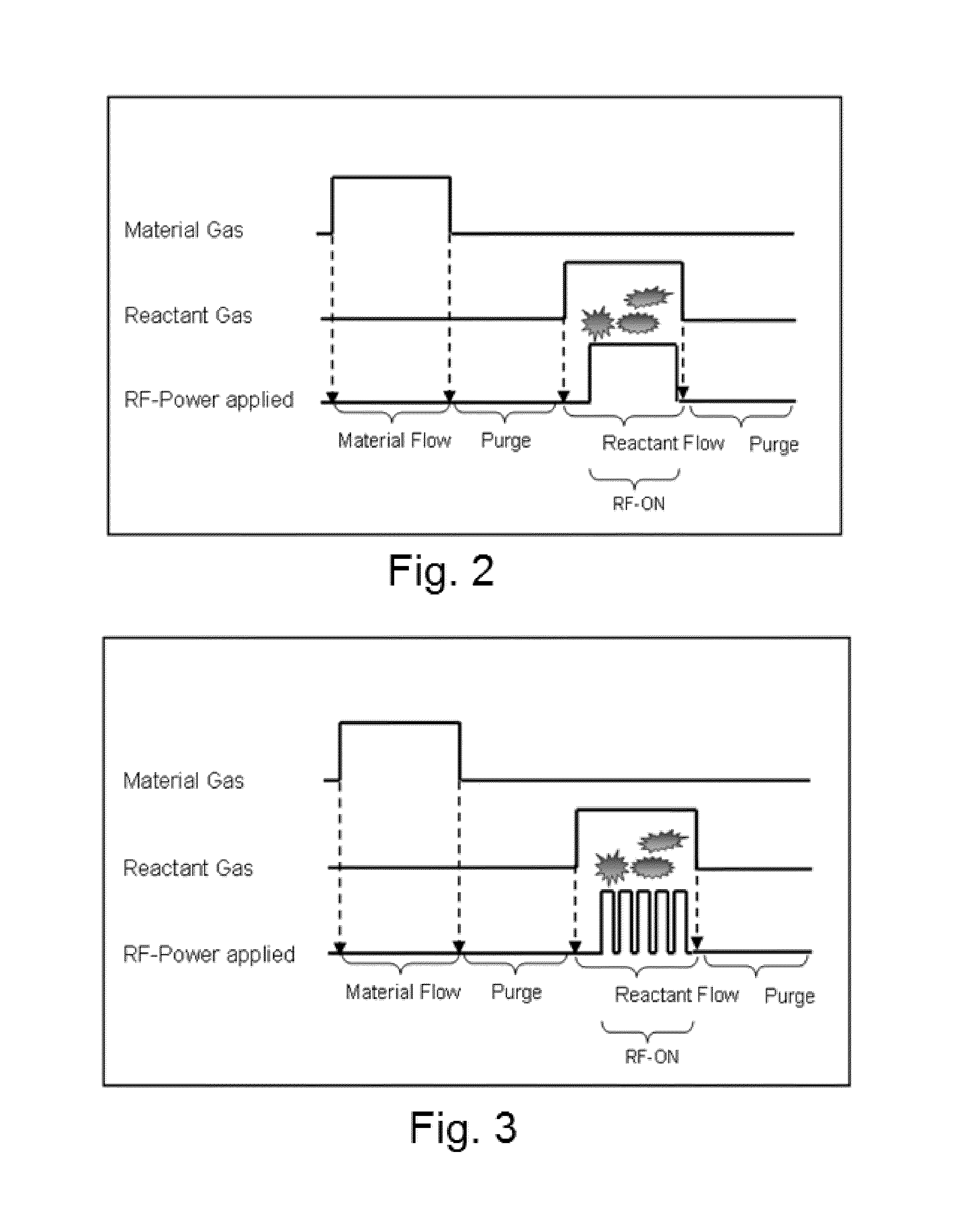
[0047]In this example, the apparatus shown in the schematic diagram of FIG. 1 was used to form a film. This apparatus comprises a reactor11 which can be retained in a vacuum state, susceptor 1 with heating mechanism used to hold a single wafer on top, shower head 2 which provides a mechanism for supplying gas, RF application mechanism 5 that generates a pulse-time-modulated plasma between the shower head and susceptor, precursor gas supply line 8 equipped with an open / close valve 3 connected to the shower head 2, reactant gas supply line 9 equipped with another open / close valve 4, exhaust line 10 used to exhaust the atmosphere inside the reactor 11, and vacuum pump 6 connected after the exhaust line via a pressure control valve 7, among others. Note that a purge gas line (not illustrated) is also connected to the shower head 2 just like the reactant gas supply line 9.

[0048]A Si wafer (300 mm in diameter) was heated to 70° C., and then N,N,N′,N′-tetraethylsilanediamine (SAM24) being ...


PUM

PropertyMeasurementUnit
pressureaaaaaaaaaa
pulse-time-modulationaaaaaaaaaa
thicknessaaaaaaaaaa

Abstract

A thin film is formed by alternating multiple times, respectively, a process of adsorbing a precursor onto a substrate and a process of treating the adsorbed surface using a reactant gas and a plasma, wherein the reactant gas is supplied substantially uniformly over the substrate, and the plasma is pulse-time-modulated and applied in the process of supplying the reactant gas.

Description

BACKGROUND[0001]1. Field of the Invention[0002]The present invention generally relates to a method of depositing a film by atomic layer deposition (ALD); particularly to a method of depositing a film by ALD with pulse-time-modulated plasma.[0003]2. Description of the Related Art[0004]Plasma Enhanced Atomic Layer Deposition (PE-ALD) is one of the plasma deposition processes. This method forms a film by repeating a process of adsorbing a precursor on a wafer and a process of treating the adsorbed precursor with a reactant gas plasma wherein the reactant gas plasma reacts the precursor adsorbed on the surface, thereby forming an atomic sub-layer on the wafer in each cycle of the repeating processes. To deposit a thick film, it requires a cyclic deposition of at least several hundred times, taking a long time to complete the deposition process. In the above, since plasma treatment is repeated at least several hundred times, surface potential on the wafer increases as a result of accumul...

Claims


Application Information

Patent Timeline
Patent Type & Authority Patents(United States)
IPC IPC(8): C23C16/56C23C16/515
CPCC23C16/325C23C16/345C23C16/40C23C16/401C23C16/45536C23C16/45542
Inventor UEDA, SHINTARO
Owner ASM JAPAN
Why Eureka
Try Eureka