SOI substrate and manufacturing method thereof

a technology of silicon insulator and substrate, which is applied in the direction of semiconductor devices, electrical equipment, basic electric elements, etc., can solve the problems of inner pressure, crack generation, and increase of embrittlement layer, and achieve the effect of less surface roughness and improved yield of semiconductor devices

Inactive Publication Date: 2013-07-02
SEMICON ENERGY LAB CO LTD
View PDF51 Cites 0 Cited by
  • Summary
  • Abstract
  • Description
  • Claims
  • Application Information

AI Technical Summary

Benefits of technology

[0016]In one embodiment of the invention, a trigger for separating the semiconductor layer is the temperature difference in the heating. Therefore, a region which triggers the separation does not need to be formed; thus, the number of steps for manufacturing an SOI substrate can be reduced.
[0038]According to the present invention, an SOI substrate having a semiconductor layer with less surface roughness can be provided. With the semiconductor layer of the SOI substrate, yield of a semiconductor device can be improved.

Problems solved by technology

In other words, hydrogen microbubbles are generated when the single crystal silicon substrate including an embrittlement layer is heated, and then, the volume of the embrittlement layer expands and inner pressure of the embrittlement layer increases; accordingly, a crack is generated.
Accordingly, there is a problem in that surface of the silicon layer separated along the embrittlement layer is not a mirror-flat surface of the like practically; thus, planarity of the surface is deteriorated.

Method used


Image

  • SOI substrate and manufacturing method thereof
  • SOI substrate and manufacturing method thereof
  • SOI substrate and manufacturing method thereof

Examples


embodiment 1

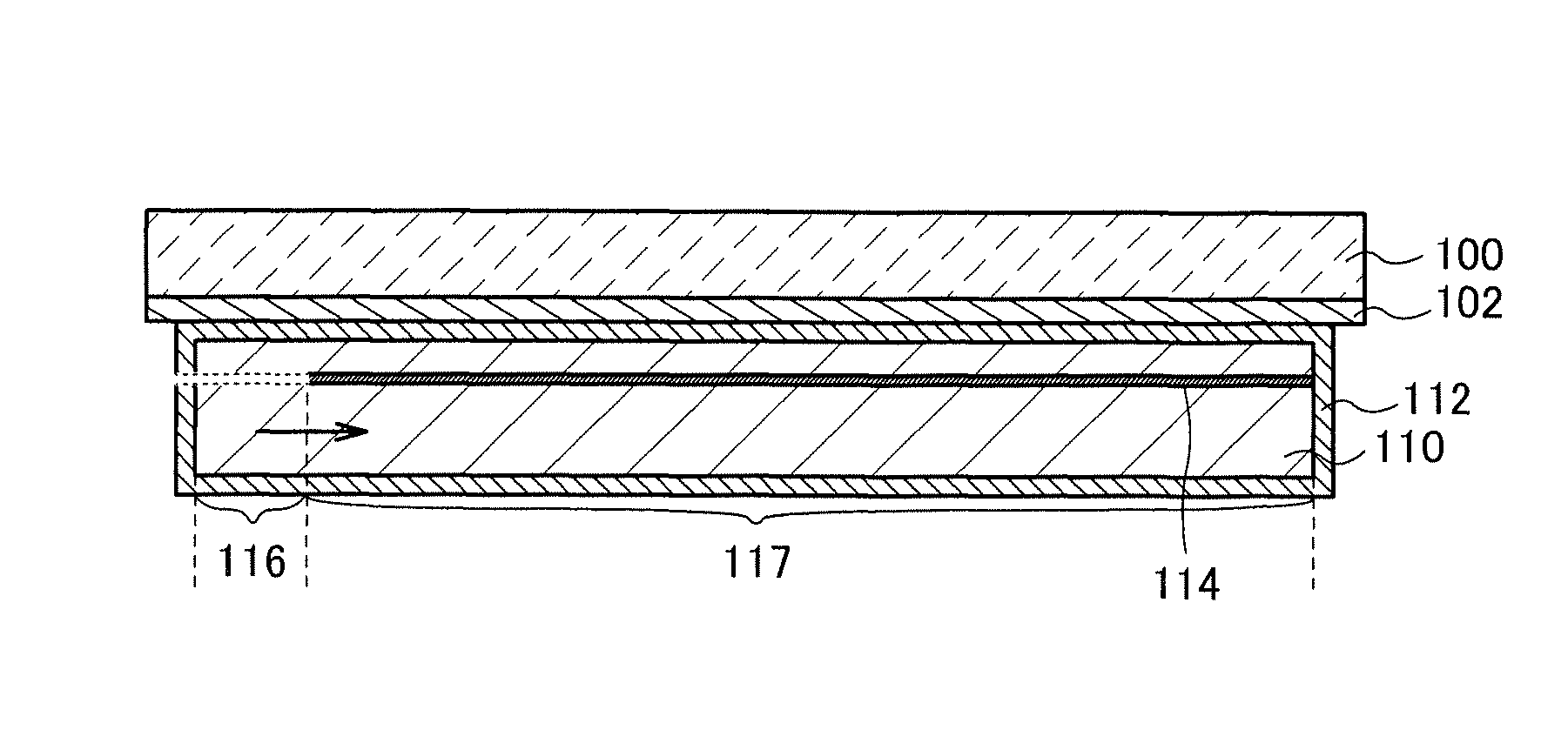
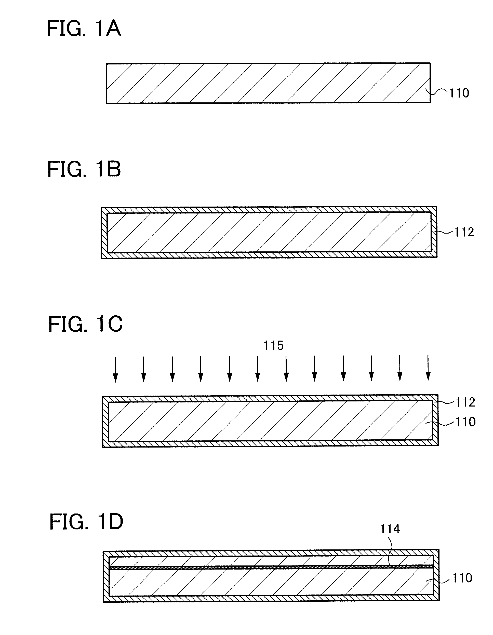
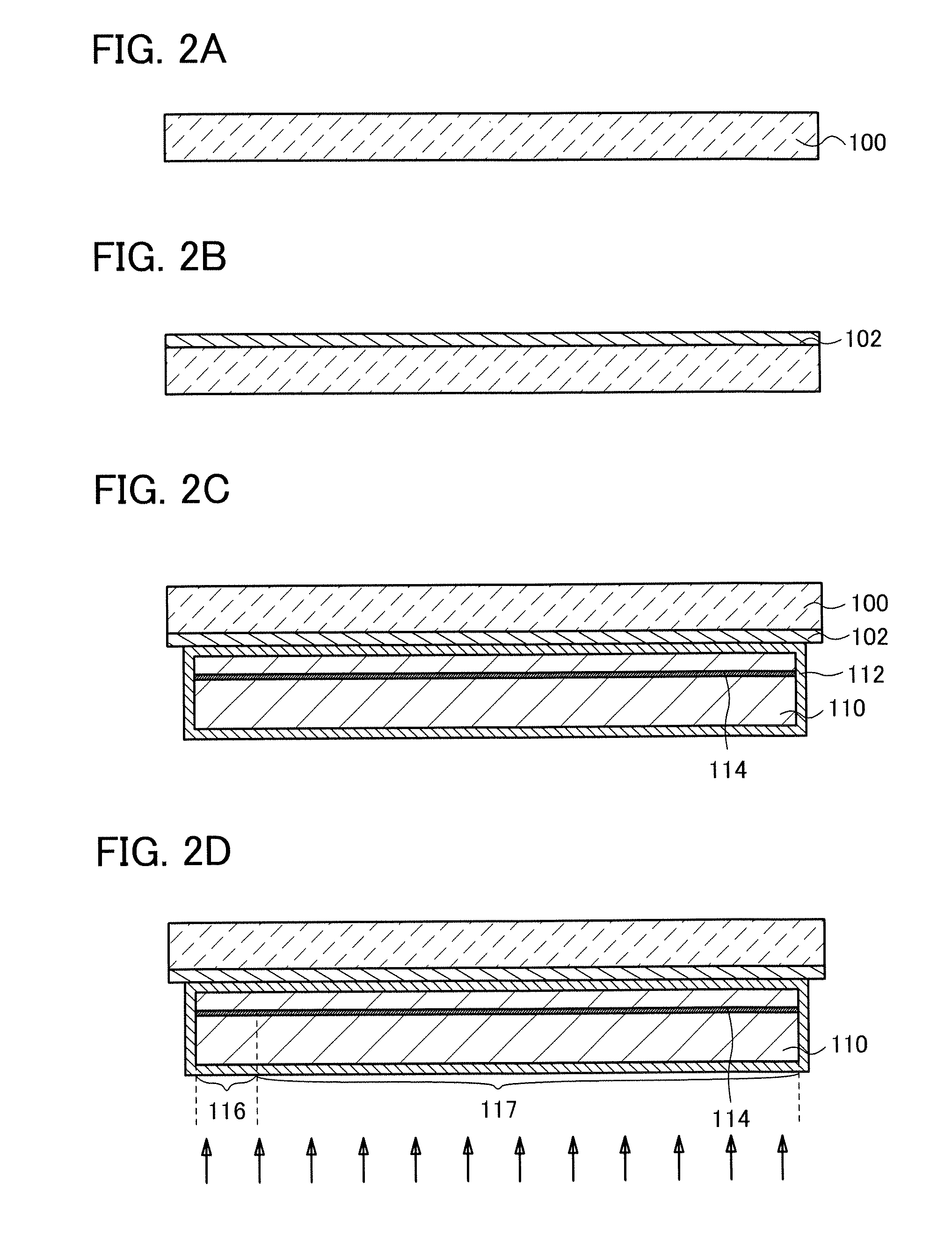
[0059]In this embodiment, an example of a manufacturing process of an SOI substrate will be described with reference to FIGS. 1A to 1D, FIGS. 2A to 2D, and FIGS. 3A to 3D. Specifically, an SOI substrate in which a single crystal semiconductor layer is provided over a base substrate and a manufacturing method thereof will be described.

[0060]First, a bond substrate is prepared. In this embodiment, a single crystal semiconductor substrate 110 is used as the bond substrate (see FIG. 1A).

[0061]Note that in this embodiment, after the bond substrate is processed, the base substrate is processed; however, an embodiment of the disclosed invention is not construed as being limited thereto. Alternatively, the base substrate may be processed first, or the bond substrate may be processed at the same time as the base substrate.

[0062]As the single crystal semiconductor substrate 110, a single crystal semiconductor substrate formed with an element belonging to Group 14 of the periodic table, such a...

embodiment 2

[0096]In this embodiment, an example of a manufacturing method of an SOI substrate which is different from Embodiment 1 will be described with reference to FIGS. 8A to 8C and FIGS. 9A and 9B. The manufacturing method of the SOI substrate according to this embodiment is common to that of Embodiment 1 in many points, and thus detailed description of the same points will be omitted.

[0097]As treatments for the single crystal semiconductor substrate 110 as the bond substrate, the same process described using FIGS. 1A to 1D and in the description thereof in the Embodiment 1 is performed first. Embodiment 1 can be referred to for the details.

[0098]As for the base substrate 100, the process up to and including formation of the nitrogen-containing layer 102 over the base substrate 100 is carried out on the basis of FIGS. 2A and 2B and the description thereof in Embodiment 1.

[0099]Next, in the same manner to Embodiment 1, the surface of the base substrate 100 and the surface of the single cry...

embodiment 3

[0108]In this embodiment, a manufacturing method of a semiconductor device using the SOI substrate according to the aforementioned embodiments will be described with reference to FIGS. 10A to 10E, FIGS. 11A to 11D, and FIG. 12. In this embodiment, a manufacturing method of a semiconductor device including a plurality of transistors will be described as an example of the semiconductor device. Various semiconductor devices can be formed with the use of transistors described below in combination.

[0109]FIG. 10A is a cross-sectional view illustrating a part of the SOI substrate manufactured using the method described in aforementioned embodiments (for example, see FIG. 3D or 9B).

[0110]A semiconductor layer 141 corresponds to the single crystal semiconductor layer 119 in FIG. 3D and the single crystal semiconductor layer 139 in FIG. 9B. The semiconductor layer 141 includes a region 142 having surface roughness. The region 142 corresponds to the region 116 and the region 136 from which the...


PUM

PropertyMeasurementUnit
temperatureaaaaaaaaaa

Abstract

A bond substrate is irradiated with ions, so that an embrittlement layer is formed, then, the bond substrate is bonded to a base substrate. Next, a part of a region of the bonded bond substrate is heated at a temperature higher than a temperature of the other part of the region of the bond substrate, or alternatively, a first heat treatment is performed on the bonded bond substrate as a whole at a first temperature; and a second heat treatment is performed on a part of a region of the bonded bond substrate at a second temperature higher than the first temperature, so that separation of the bond substrate proceeds from the part of the region of the bond substrate to the other part of the region of the bond substrate in the embrittlement layer. Accordingly, a semiconductor layer is formed over the base substrate.

Description

BACKGROUND OF THE INVENTION[0001]1. Field of the Invention[0002]One embodiment of the disclosed invention relates to a silicon on insulator (SOI) substrate and a manufacturing method thereof.[0003]2. Description of the Related Art[0004]In recent years, a silicon on insulator (SOI) substrate that includes a thin single crystal silicon layer on an insulating surface has been developed instead of a bulk silicon wafer.[0005]As an example of a method for manufacturing an SOI substrate, the following method can be given. Hydrogen ions are added to a single crystal silicon substrate so that an embrittlement layer (also referred to as a separation layer) is formed. A base substrate (for example a glass substrate) and the single crystal silicon substrate are bonded to each other. The bonded single crystal silicon substrate is heated so that a thin single crystal layer is separated along the embrittlement layer; accordingly, a thin single crystal layer is formed over the base substrate (see P...

Claims


Application Information

Patent Timeline
Patent Type & Authority Patents(United States)
IPC IPC(8): H01L21/762H01L29/02
CPCH01L21/762H01L29/02H01L21/76254H01L27/1266H01L29/66772H01L21/84
Inventor OKUNO, NAOKITOKUNAGA, HAJIME
Owner SEMICON ENERGY LAB CO LTD
Why Eureka
Try Eureka