Roll-to-roll digital photolithography

a digital photolithography and roll-to-roll technology, applied in the field of photolithography, can solve the problems of distortion of the substrate, unavoidable alignment errors, and limitations of the existing roll-to-roll photolithography system to produce flexible multi-layered circuits

Inactive Publication Date: 2013-07-16
3M INNOVATIVE PROPERTIES CO
View PDF11 Cites 4 Cited by
  • Summary
  • Abstract
  • Description
  • Claims
  • Application Information

AI Technical Summary

Benefits of technology

[0012]The presently disclosed techniques allow for dramatically enhanced functionality and performance in thin-film flexible circuits that are manufactured using roll-to-roll processes. Exemplary flexible circuit devices include high-resolution active matrix display backplanes with integrated row and column drivers, pixel drivers for active-matrix OLED displays, and highly functional radio frequency identification (RFID) products, for example.

Problems solved by technology

We have now recognized that existing roll-to-roll photolithography systems are limited in their ability to produce flexible multilayered circuits with consistently small layer-to-layer alignment errors, as a result of physical distortions of the underlying polymer substrate or web during fabrication.
This limitation has a direct effect on the minimum size of some features that can be used in the flexible multilayered circuit.
For example, during processing of thin-film integrated circuits on polymer substrates, a number of phenomena can cause distortions of the substrate.
When practicing traditional photolithography even on relatively small pieces of polymer substrate, these and other distortions can result in unavoidable alignment errors of over 20 μm on a circuit that is only 125 mm across.
However, those techniques may not be practical for more complex or higher performance circuits.

Method used


Image

  • Roll-to-roll digital photolithography
  • Roll-to-roll digital photolithography
  • Roll-to-roll digital photolithography

Examples


Embodiment Construction

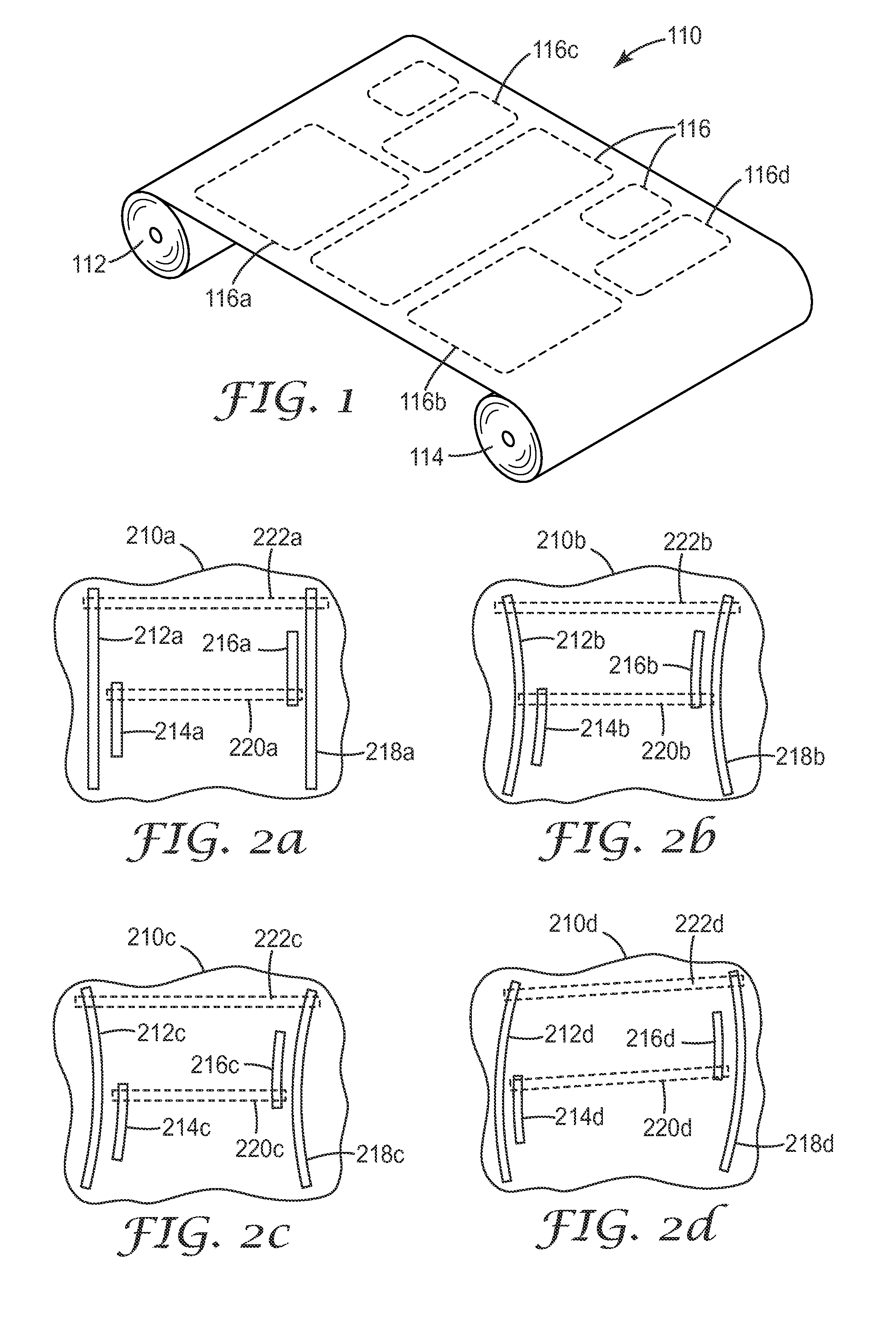
[0032]In FIG. 1 we see in perspective schematic view a roll of flexible multilayered circuit film 110 partially unrolled and distributed between a first roll 112 and a second roll 114. The film 110 has a flexible substrate and a plurality of patterned circuit layers formed thereon. The circuit layers may form a single circuit design that extends from one end of the film 110, on roll 112, to the opposite end of the film 110, on roll 114. More typically, the circuit layers form a plurality of discrete multilayered circuits that are located in distinct areas or zones 116 of the film 110. In some cases, some or all of these discrete circuits can be later separated from each other by converting operations such as cutting the roll of film into corresponding discrete pieces or parts. The discrete circuits in zones 116 may all have nominally the same circuit layout, intended for the same end-use application, or only some may have the same circuit layout, or they may all have different circu...


PUM

PropertyMeasurementUnit
flexibleaaaaaaaaaa
photosensitiveaaaaaaaaaa
speedaaaaaaaaaa

Abstract

Methods of making flexible circuit films include providing a polymer film or other flexible substrate having a plurality of alignment marks and a photosensitive material thereon. The substrate passes around a suitable roller, belt, or other inelastic conveyor such that the substrate and the conveyor move together at least from a first location to a second location. Positions of a first set of the alignment marks on a first portion of the substrate are measured when such portion is at the first location, and the measured positions can be used to calculate a distortion of the substrate. The photosensitive material is then patternwise exposed when the first portion of the substrate has moved to the second location. The patternwise exposing is based on the measured positions of the first set of alignment marks, and may include exposing the web with a distortion-adjusted pattern. Related systems and articles are also disclosed.

Description

CROSS REFERENCE TO RELATED APPLICATIONS[0001]This application is a national stage filing under 35 U.S.C. 371 of PCT / US2009 / 068426, filed on Dec. 17, 2009, which claims priority to U.S. Provisional Application No. 61 / 140,248, filed on Dec. 23, 2008, the disclosure of which is incorporated by reference in its / their entirety herein.FIELD OF THE INVENTION[0002]This invention relates generally to photolithography, with particular application to photolithography used to make multilayered circuits on flexible substrates. The invention also relates to related articles, systems, and methods.BACKGROUND[0003]Flexible circuits that feature multiple layers or levels of circuit traces formed on a flexible substrate are known. Reference is made, for example, to U.S. Patent Application Publication US 2008 / 0205010 (Haase). The flexible circuit is formed by building up on the flexible substrate, layer-by-layer, a series of electrically conducting, semiconducting and insulating layers and patterning e...

Claims


Application Information

Patent Timeline
Patent Type & Authority Patents(United States)
IPC IPC(8): G03F9/00
CPCG03F7/22G03F7/70791G03F9/7003G03F7/70516H05K3/0082H05K3/0008H05K1/0269H05K1/0393H05K2201/09918H05K2203/1545H05K2203/163H05K2203/166
Inventor HAASE, MICHAEL A.TOKIE, JEFFREY H.THEIS, DANIEL J.NELSON, BRIAN K.
Owner 3M INNOVATIVE PROPERTIES CO
Why Eureka
Try Eureka