Hybrid substrateless device with enhanced tuning efficiency

a substrateless optical device and enhanced technology, applied in the direction of optical waveguide light guide, semiconductor/solid-state device details, radiation controlled devices, etc., can solve the problems of increasing the risk of cds variation in optical ring circuits, and consuming significant power in thermal tuning, so as to improve the thermal tuning efficiency of the substrateless optical device, improve device performance, and improve the effect of device performan

Active Publication Date: 2014-08-05
ORACLE INT CORP
View PDF5 Cites 4 Cited by
  • Summary
  • Abstract
  • Description
  • Claims
  • Application Information

AI Technical Summary

Benefits of technology

[0009]One embodiment of the present disclosure provides a hybrid integrated module. This hybrid integrated module may include a semiconductor die mechanically coupled face-to-face to an integrated device in which the substrate has been removed. For example, the integrated circuit may include an optical device (such as a wavelength-selective element or filter, a signal modulating element, or a light detecting element) fabricated on a silicon-on-insulator (SOI) wafer in which the backside silicon handler has been completely removed, thereby facilitating improved device performance and highly efficient thermal tuning of the operating wavelength of the optical device. Moreover, the semiconductor die may be a VLSI chip that provides power, and serves as a mechanical handler and / or an electrical driver. The thermal tuning efficiency of the substrateless optical device may be enhanced by over 100× relative to an optical device with an intact substrate, and by 5× relative to an optical device in which the substrate has only been removed in proximity to the optical device.
[0010]This architecture may also facilitate large-scale integration of hybrid integrated modules into a multi-chip module (MCM) that includes a larger bonded 2-dimensional array, in which the integrated devices in the hybrid integrated modules are optically coupled by optical couplers (such as diffraction grating couplers), which may be immediately optically accessible through the backside of the photonic layer because the silicon substrate has been removed. These arrays may enhance functionality and performance over a single-bonded hybrid integrated module, while ensuring high thermal tuning efficiency.
[0011]Moreover, properly arranged metal and / or dielectrics in or on the integrated device(s) may be used to form an optical mirror and / or to improve the optical coupling efficiency between the optical couplers.
[0013]Additionally, in some embodiments the integrated circuit includes a semiconductor layer and an oxide layer, and an electro-optic material disposed on the back surface of the oxide layer, thereby facilitating tuning, routing or guiding of an optical signal in the optical device.

Problems solved by technology

However, optical ring circuits are more susceptible to variations in CDs, even when they are fabricated using the same CMOS tool set and manufacturing standards.
However, depending on the device design, thermal tuning can consume significant power.

Method used


Image

  • Hybrid substrateless device with enhanced tuning efficiency
  • Hybrid substrateless device with enhanced tuning efficiency
  • Hybrid substrateless device with enhanced tuning efficiency

Examples


Embodiment Construction

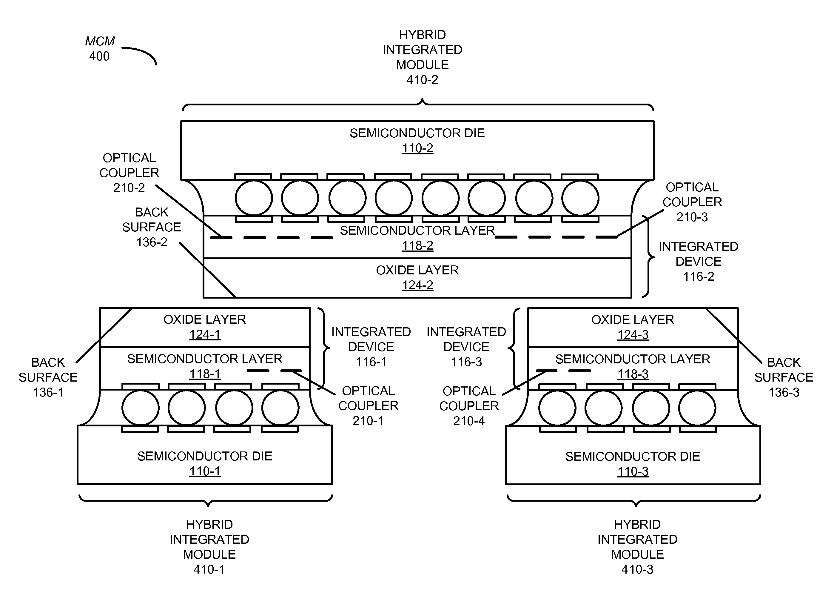
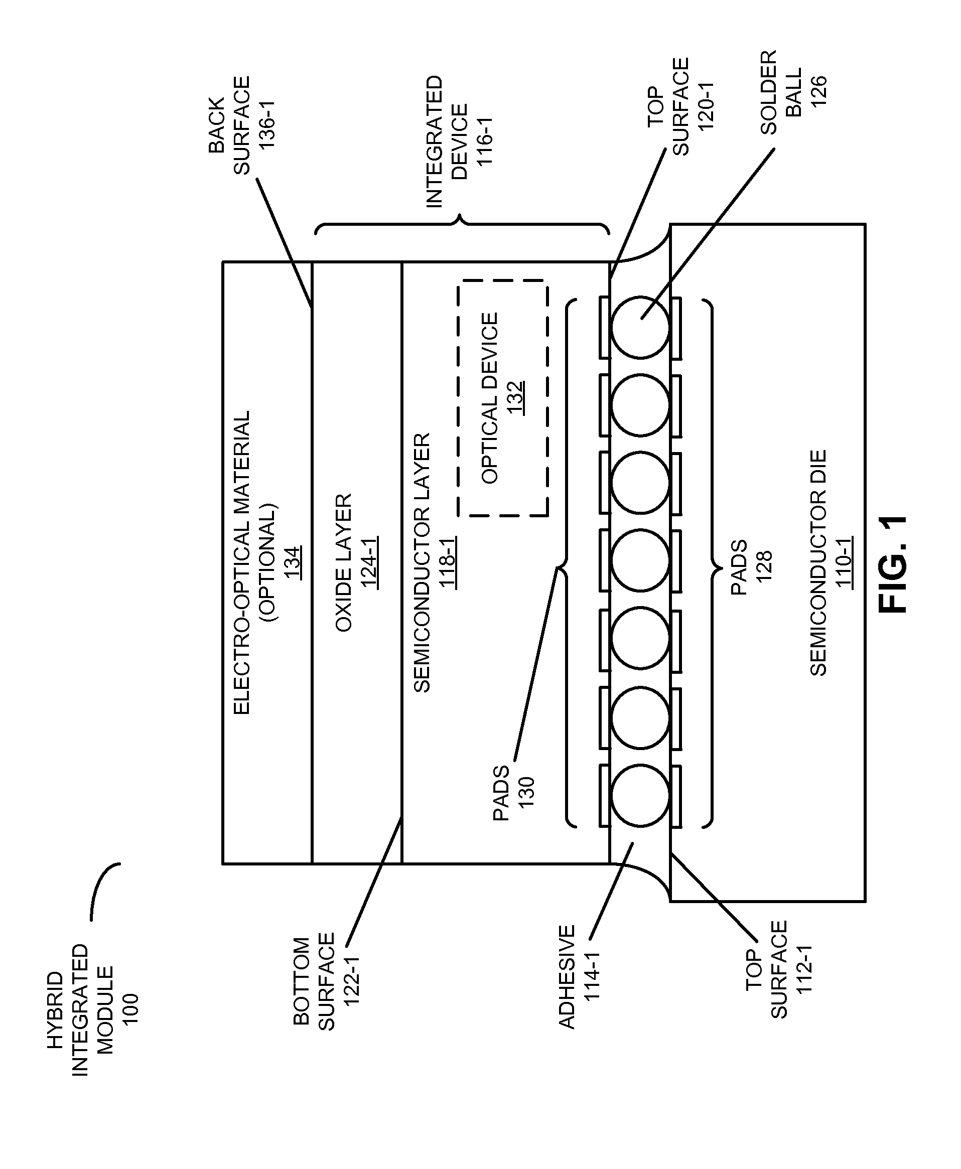
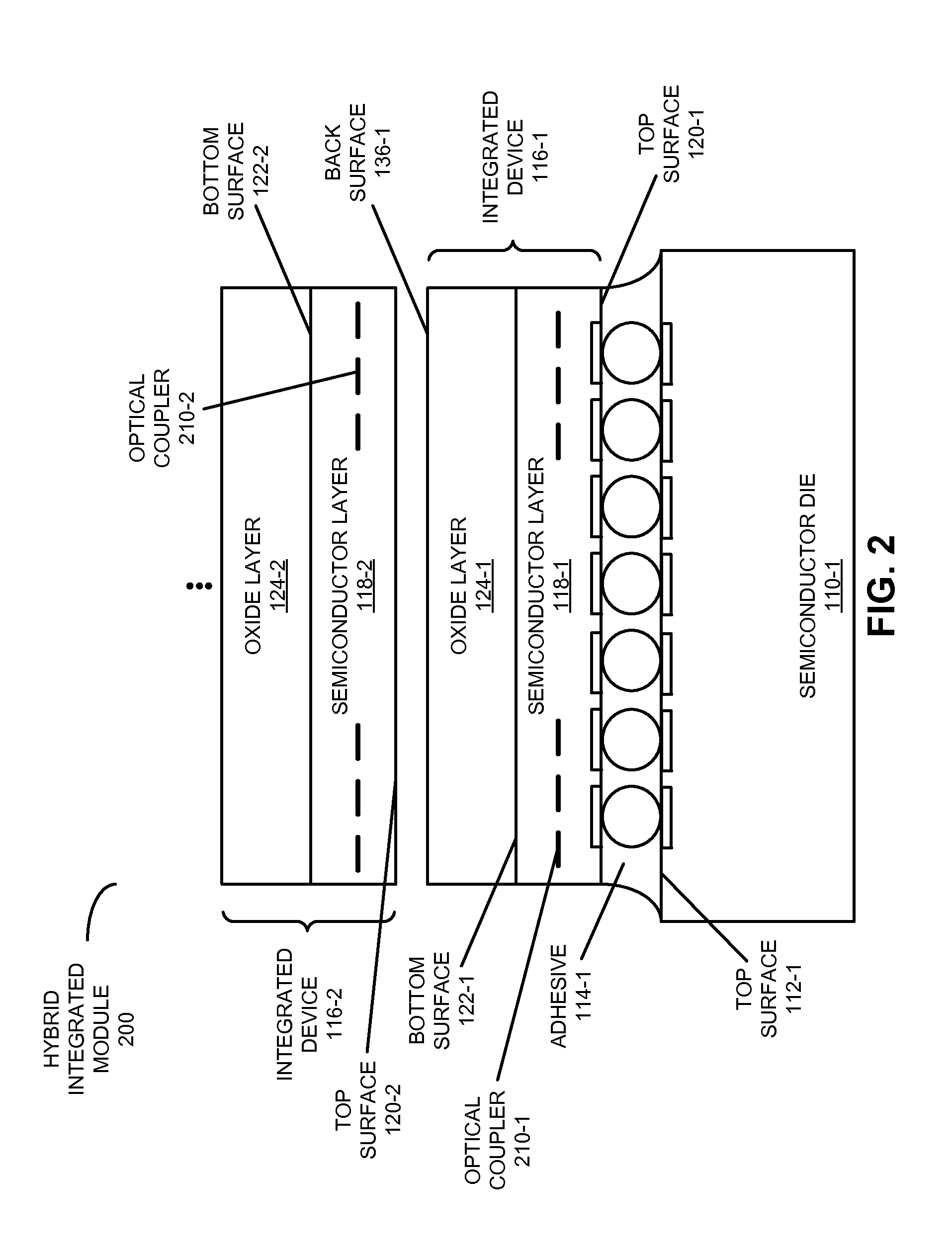
[0024]FIG. 1 presents a block diagram of a hybrid integrated module 100. This hybrid integrated module includes: a semiconductor die 110-1 having a top surface 112-1; an adhesive 114-1 (such as epoxy) mechanically coupled to top surface 112-1 of semiconductor die 110-1; and an integrated device 116-1. Moreover, integrated device 116-1 includes: a semiconductor layer 118-1 having a top surface 120-1 and a bottom surface 122-1, where top surface 120-1 is mechanically coupled to adhesive 114-1, so that semiconductor layer 118-1 and semiconductor die 110-1 are mounted face-to-face; and an oxide layer 124-1 disposed on bottom surface 122-1.

[0025]In addition to the mechanical coupling provided by adhesive 114-1, hybrid integrated module 100 may include solder balls, such as solder ball 126 (e.g., bondline micro-bumps or micro-solder), electrically coupling pads 128 on top surface 112-1 and pads 130 on top surface 120-1, where adhesive 114-1 at least in part fills a space between top surfa...


PUM


Abstract

In a hybrid integrated module, a semiconductor die is mechanically coupled face-to-face to an integrated device in which the substrate has been removed. For example, the integrated circuit may include an optical device fabricated on a silicon-on-insulator (SOI) wafer in which the backside silicon handler has been completely removed, thereby facilitating improved device performance and highly efficient thermal tuning of the operating wavelength of the optical device. Moreover, the semiconductor die may be a VLSI chip that provides power, and serves as a mechanical handler and / or an electrical driver. The thermal tuning efficiency of the substrateless optical device may be enhanced by over 100× relative to an optical device with an intact substrate, and by 5× relative to an optical device in which the substrate has only been removed in proximity to the optical device.

Description

GOVERNMENT LICENSE RIGHTS[0001]This invention was made with Government support under Agreement No. HR0011-08-9-0001 awarded by DARPA. The Government has certain rights in the invention.BACKGROUND[0002]1. Field[0003]The present disclosure relates to integrated modules. More specifically, the present disclosure relates to a hybrid integrated module that includes a semiconductor die mechanically coupled to an integrated device in which the substrate has been removed.[0004]2. Related Art[0005]The operating wavelengths of optical components, such as ring modulators, eschelle grating and ring-filtering devices, often differ from their target values. Origins of this difference include: process variability, manufacturing tolerances, and wafer thickness variations (notably, in the silicon device layer of silicon-on-insulator or SOI wafers). In the case of ring-resonator filters, these factors can affect the critical dimensions (CDs) of the ring resonator, with a corresponding impact on the p...

Claims


Application Information

Patent Timeline
Patent Type & Authority Patents(United States)
IPC IPC(8): H01L27/12G02B6/10H01L21/50H01L27/146H01L27/148
CPCH01L27/1465H01L27/1467H01L27/14661H01L27/14881H01L21/187H01L2224/16225H01L2224/32225H01L2224/73204H01L2224/73253H01L2924/00
Inventor SHUBIN, IVANKRISHNAMOORTHY, ASHOK V.CUNNINGHAM, JOHN E.
Owner ORACLE INT CORP
Why Eureka
Try Eureka