Deep-ultraviolet light source capable of stopping leakage of harmful X-rays

a technology of ultraviolet light and harmful x-rays, applied in the field of deep ultraviolet light sources, can solve the problems of low ultraviolet emission efficiency, large electromagnetic noise, and preferable in view of eco-efficiency, and achieve the effect of reducing the required degree of vacuum scaling, and prolonging the life of electron emission sources

Active Publication Date: 2013-07-16
STANLEY ELECTRIC CO LTD
View PDF7 Cites 5 Cited by
  • Summary
  • Abstract
  • Description
  • Claims
  • Application Information

AI Technical Summary

Benefits of technology

[0027]Further, a 30 to 60 nm thick aluminum metal back layer is formed on the AlxGa1-xN / AlN multiple quantum well layer. The aluminum metal back layer prevents the AlxGa1-xN / AlN multiple quantum well layer from being destroyed due to the electrostatic charges thereof.
[0028]Furthermore, a thickness of the AlxGa1-xN / AlN multiple quantum well layer is 300 to 400 nm, and the energy of the electron beam is 6 to 7 keV. Thus, the ultraviolet emission efficiency becomes maximum.
[0029]An electron emission source including a graphite nanometer-order or submicrometer-order needle rod for generating the electron beam is provided. Thus, the required degree of vacuum of a vacuum scaling is decreased, and the lifetime of the electron emission source becomes longer.
[0030]According to the presently disclosed subject matter, the leakage of harmful X-rays can be stopped.

Problems solved by technology

In the above-described first prior art deep-ultraviolet light source, however, since harmful mercury is included, it is not preferable in view of eco-efficiency.
Still further, the ultraviolet emission efficiency is low.
Finally, since the drive voltage is high, the electromagnetic noise is large.
However, the above-described second prior art deep-ultraviolet light source still has the same disadvantages as in the first prior art deep-ultraviolet light source except for the ultraviolet emission efficiency.
In the above described third prior art deep-ultraviolet light source, obtained ultraviolet emission intensity is high due to the high pressure of mercury gas; however, the ultraviolet emission efficiency is low because the conversion efficiency from the input electric power to the ultraviolet emission energy is low.
Further, since a circuit for generating a high voltage discharge is required, this deep-ultraviolet light source is high in cost.
Still further, in the same way as in the first prior art deep-ultraviolet light source, since harmful mercury is included, it is not preferable in view of eco-efficiency, and since the drive voltage is high, the electromagnetic noise is large.
In the above-described fourth prior art deep-ultraviolet light source, however, since the self-absorption of light is large and the rate of radiation recombination is small, the ultraviolet emission efficiency is low.
The above-described fifth prior art deep-ultraviolet light source, however, has the following problems.
Firstly, the MQW layer pumped by art electron beam generates a harmful X-ray in addition to the deep-ultraviolet light.
Secondly, since the MQW layer has poor conductivity, irradiation of the MQW layer with an electron beam for even a short time period would electrostatically destroy the MQW layer.
Thirdly, the ultraviolet emission efficiency is still low.
Fourthly, an electron emission source for generating an electron beam may be a thermal electron emission source such as a tungsten (W) filament or a cold-cathode electron emission source such as carbon nanotubes (CNTs), however, such an electron emission source has a short lifetime such as 1000 hours.
As a result, this deep-ultraviolet light source has a short lifetime.
Also, since the thermal electron emission source requires heating power, the ultraviolet emission efficiency would be low.
On the other hand, since the cold-cathode electron emission source requires a high vacuum sealing, the manufacturing cost would become high.

Method used


Image

  • Deep-ultraviolet light source capable of stopping leakage of harmful X-rays
  • Deep-ultraviolet light source capable of stopping leakage of harmful X-rays
  • Deep-ultraviolet light source capable of stopping leakage of harmful X-rays

Examples


Embodiment Construction

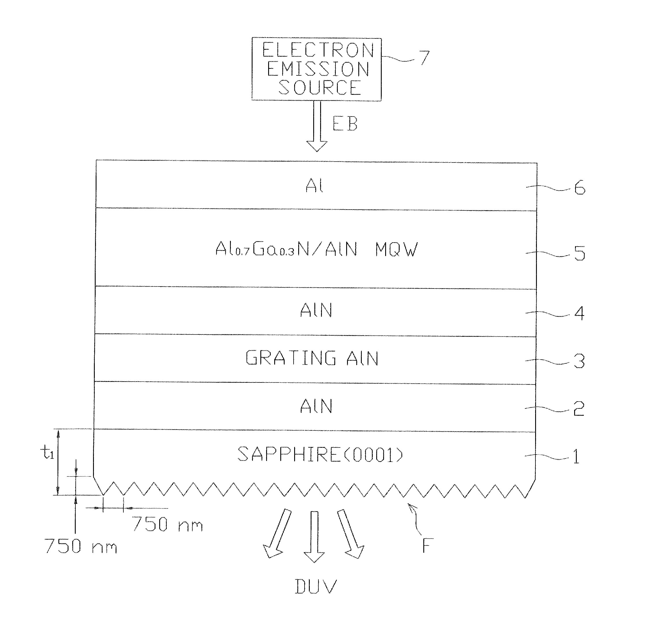
[0048]In FIG. 1, which illustrates an embodiment of the deep-ultraviolet light source according to the presently disclosed subject matter, this deep ultraviolet light source is constructed by a sapphire (0001) substrate 1, an about 600 nm thick AlN buffer layer 2 formed on the sapphire (0001) substrate 1, an about 3 μm thick grating AlN layer 3 formed on the AlN buffer layer 2, an about 60 nm thick Al0.7Ga0.3N / AlN MQW layer 5 consisting of ten periods of one about 3 nm thick Al0.7Ga0.3N well layer and one about 3 nm thick AlN barrier layer, and an aluminum (Al) metal back layer 6.

[0049]In FIG. 1, when the deep-ultraviolet light source of FIG. 1 is irradiated with an electron beam EB emitted from an electron emission source 7, a deep-ultraviolet light DUV is emitted from a light taken-out surface F of the sapphire (0001) substrate 1.

[0050]First, the sapphire (0001) substrate 1 is discussed in detail below.

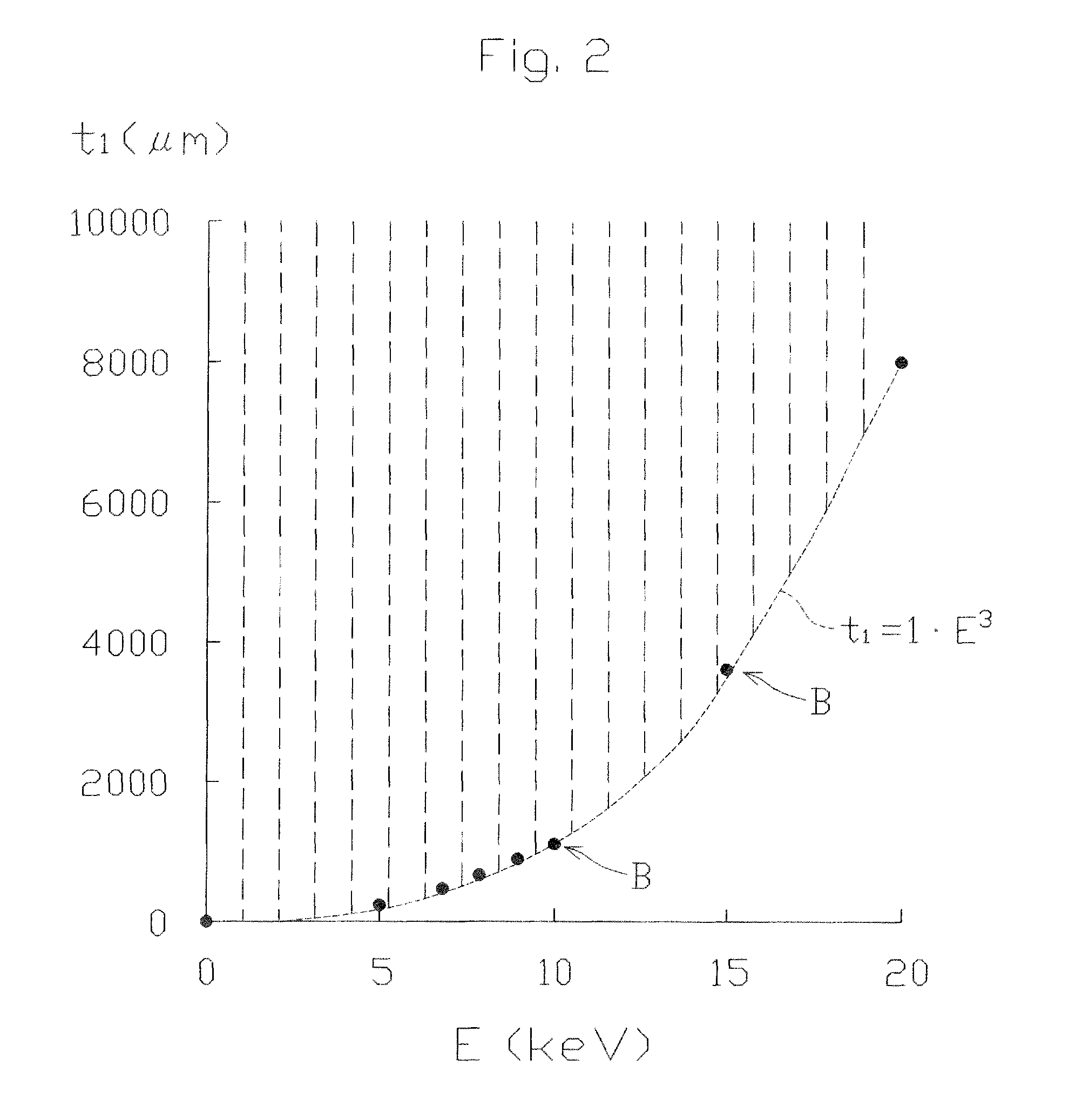
[0051]In FIG. 2, each black spot B designates a simulated thickness t1 of the s...


PUM


Abstract

In a deep-ultraviolet tight source includes sapphire substrate, a wide band gap semiconductor layer having a wavelength smaller than 300 nm, formed on the sapphire substrate, and en electron beam source for irradiating the wide band gap semiconductor layer with an electron beam. The wide band gap semiconductor layer is configured to be irradiated with the electron beam to emit deep-ultraviolet light through the sapphire substrate. A thickness t1 of the sapphire substrate satisfies: t1≧α·E3 is an energy of the electron beam (keV); and α is 1 μm / (keV)3.

Description

[0001]This application claims the priority benefit under 35 U.S.C. §119 to Japanese Patent Application No. JP2011-063651 filed on Mar. 23, 2011, which disclosure is hereby incorporated in its entirety by reference.BACKGROUND[0002]1. Field[0003]The presently disclosed subject matter relates to deep-ultraviolet light source used for various applications including disinfection, sterilization and water purification, or in semiconductor manufacturing processes and so on.[0004]2. Description or the Related Art[0005]Generally, deep-ultraviolet, light sources of an about 200 to 260 nm wavelength range have been broadly used as disinfection light sources, sterilization light sources and water purification light sources, or in semiconductor manufacturing processes.[0006]A first prior art deep-ultraviolet light source is a low pressure mercury discharge apparatus using a hot cathode (see: JP5-54857, JP5-217552 & JP6-96609). That is, an anode electrode and a cathode electrode are inserted at en...

Claims


Application Information

Patent Timeline
Patent Type & Authority Patents(United States)
IPC IPC(8): G21K5/02
CPCB82Y20/00C09K11/0883C02F1/325C09K11/64H01J1/63H01J63/04H01J63/06
Inventor MATSUMOTO, TAKAHIROIWAYAMA, SHO
Owner STANLEY ELECTRIC CO LTD
Why Eureka
Try Eureka