Stacked linear power amplifier with capacitor feedback and resistor isolation

a technology of capacitor feedback and resistor isolation, which is applied in the direction of amplifiers, amplifiers with semiconductor devices only, amplifiers with semiconductor devices, etc., can solve the problems of inacceptable linearity of amplifiers in many modern communication standards, and achieve the effects of minimizing non-linearity generation, minimizing distortion, and maximizing

Active Publication Date: 2013-07-16
PSEMI CORP
View PDF58 Cites 132 Cited by
  • Summary
  • Abstract
  • Description
  • Claims
  • Application Information

AI Technical Summary

Benefits of technology

[0010]According to a first aspect, a power amplifier circuit is provided, comprising: a first field effect transistor, wherein i) an RF input signal terminal is adapted to be coupled to a gate electrode of the first field effect transistor and ii) a first DC control voltage input is adapted to be coupled to the gate electrode of the first field effect transistor; one or more additional serially connected field effect transistors serially connected among themselves and to the first field effect transistor, each having a source terminal connected to a drain terminal of a preceding field effect transistor, wherein one or more additional DC control voltage inputs are each coupled to respective gate electrodes of the one or more additional field effect transistors, an output of the power amplifier circuit being taken on a drain electrode of the last one of the one or more additional field effect transistors; and one or more capacitors, each coupled to a respective one of the one or more additional field effect transistors, wherein the first DC control voltage input, the one or more additional DC control voltage inputs and the one or more capacitors are selected to minimize generation of non-linearities of each field effect transistor of the power amplifier circuit and to maximize, through phase alignment, cancellation of distortions between the field effect transistors of the power amplifier circuit whereby, upon minimization of non-linearities and maximization of cancellation of distortions, at least two of the first field effect transistor and the one or more additional field effect transistors are biased with different drain-source voltages Vds and / or different gate-source voltages Vgs.
[0011]According to a second aspect, a power amplifier comprising a plurality of amplifying components connected in parallel is provided, each amplifying component comprising: a) a first field effect transistor wherein a first DC control voltage input is adapted to be coupled to a gate terminal of the first field effect transistor; b) one or more additional serially connected field effect transistors serially connected among themselves and to the first field effect transistor, each having a source terminal connected to a drain terminal of a preceding field effect transistor, wherein one or more additional DC control voltage inputs are each coupled to respective gate terminals of the one or more additional field effect transistors; and c) one or more capacitors, each coupled to a respective one of the one or more additional field effect transistor wherein i) an RF input signal terminal is adapted to be coupled to the gate terminal of the first field effect transistor of each amplifying component, thus providing the power amplifier with the same input to each amplifying component; ii) an output of the power amplifier is taken on the drain terminal of the last one of the one or more additional field effect transistors of each amplifying component, thus providing the power amplifier with the same output from each amplifying component; and iii) the first DC control voltage input, the one or more additional DC control voltage inputs and the one or more capacitors of at least one amplifying component are selected to minimize generation of non-linearities of each field effect transistor of the power amplifier circuit and to maximize, through phase alignment, cancellation of distortions between the field effect transistors of the power amplifier whereby, upon minimization of non-linearities and maximization of cancellation of distortions, at least two of the first field effect transistor and the one or more additional field effect transistors of the at least one amplifying component are biased with different drain-source voltages Vds and / or different gate-source voltages Vgs.
[0012]According to a third aspect, a method for controlling DC voltage inputs and capacitance values of a power amplifier is provided, comprising: providing a first field effect transistor, wherein i) an RF input signal terminal is adapted to be coupled to a gate electrode of the first field effect transistor and ii) a first DC control voltage input is adapted to be coupled to the gate electrode of the first field effect transistor; providing one or more additional serially connected field effect transistors serially connected among themselves and to the first field effect transistor, each having a source terminal connected to a drain terminal of a preceding field effect transistor, wherein one or more additional DC control voltage inputs are each coupled to respective gate electrodes of the one or more additional field effect transistors, an output of the power amplifier circuit being taken on a drain electrode of the last one of the one or more additional field effect transistors; providing one or more capacitors, each coupled to a respective one of the one or more additional field effect transistor; and controlling the first DC control voltage input, the one or more additional DC control voltage inputs and the one or more capacitors to minimize generation of non-linearities of each field effect transistor of the power amplifier circuit and to maximize, through phase alignment, cancellation of distortions between the field effect transistors of the power amplifier circuit whereby, upon minimization of non-linearities and maximization of cancellation of distortions, at least two of the first field effect transistor and the one or more additional field effect transistors are biased with different drain-source voltages Vds and / or gate-source voltages Vgs.
[0013]According to a fourth aspect, a method for controlling DC voltage inputs and capacitance values of a power amplifier is provided, comprising: a) providing a first field effect transistor, wherein a first DC control voltage input is adapted to be coupled to a gate terminal of the first field effect transistor; b) providing one or more additional serially connected field effect transistors serially connected among themselves and to the first field effect transistor, each having a source terminal connected to a drain terminal of a preceding field effect transistor, wherein one or more additional DC control voltage inputs are each coupled to respective gate terminals of the one or more additional field effect transistors; and c) providing one or more capacitors, each coupled to a respective one of the one or more additional field effect transistor, wherein: i) an RF input signal terminal is adapted to be coupled to the gate terminal of the first field effect transistor of each amplifying component, thus providing the power amplifier with the same input to each amplifying component; and ii) an output of the power amplifier is taken on the drain terminal of the last one of the one or more additional field effect transistors of each amplifying component, thus providing the power amplifier with the same output from each amplifying component, the method further comprising d) controlling the first DC control voltage input, the one or more additional DC control voltage inputs and the one or more capacitors of at least one amplifying component to minimize generation of non-linearities of each field effect transistor of the power amplifier circuit and to maximize, through phase alignment, cancellation of distortions between the field effect transistors of the power amplifier whereby, upon minimization of non-linearities and maximization of cancellation of distortions, at least two of the first field effect transistor and the one or more additional field effect transistors of the at least one amplifying component are biased with different drain-source voltages Vds and / or gate-source voltages Vgs.
[0014]According to a fifth aspect, a system for improving linearity of an electronic circuit is provided, comprising: a sensor; a bias adjustment arrangement coupled to the sensor; a bias generator coupled to the bias adjustment arrangement; and an electronic circuit coupled to the bias generator, the power amplifier adapted to receive an input signal and to provide an output signal to a load, wherein the bias adjustment arrangement controls bias values to be generated by the bias generator and fed to the electronic circuit by reducing non-linearity of the output signal of the electronic circuit through action on parameters on which the non-linearity of the output signal depends.
[0015]According to a sixth aspect, a system for improving linearity of a power amplifier is provided, comprising: a sensor; a bias adjustment arrangement coupled to the sensor; a bias generator coupled to the bias adjustment arrangement; and a power amplifier coupled to the bias generator, the power amplifier adapted to receive an input signal and to provide an output signal to a load, wherein the bias adjustment arrangement controls bias values to be generated by the bias generator and fed to the power amplifier by reducing non-linearity of the output signal of the power amplifier through action on parameters on which the non-linearity of the output signal depends, and wherein the power amplifier comprises the power amplifier defined in the previous second aspect above.

Problems solved by technology

However, in all of the above prior art examples of PA design, maximum available power appears to be the main concern.
Therefore, while the above-described power amplifiers deliver the maximum available power, the linearity of the amplifiers is unfortunately unacceptable for many modern communication standards.
Non-linearity of the PA components is one of the main causes of power spillover, because it generates harmonics of the center frequency and produces intermodulation distortion (IMD).

Method used


Image

  • Stacked linear power amplifier with capacitor feedback and resistor isolation
  • Stacked linear power amplifier with capacitor feedback and resistor isolation
  • Stacked linear power amplifier with capacitor feedback and resistor isolation

Examples


first embodiment

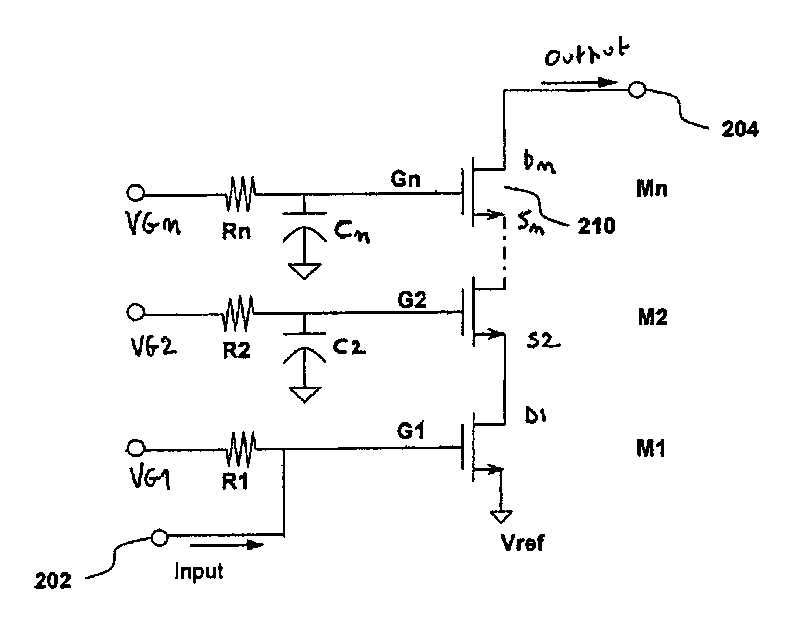
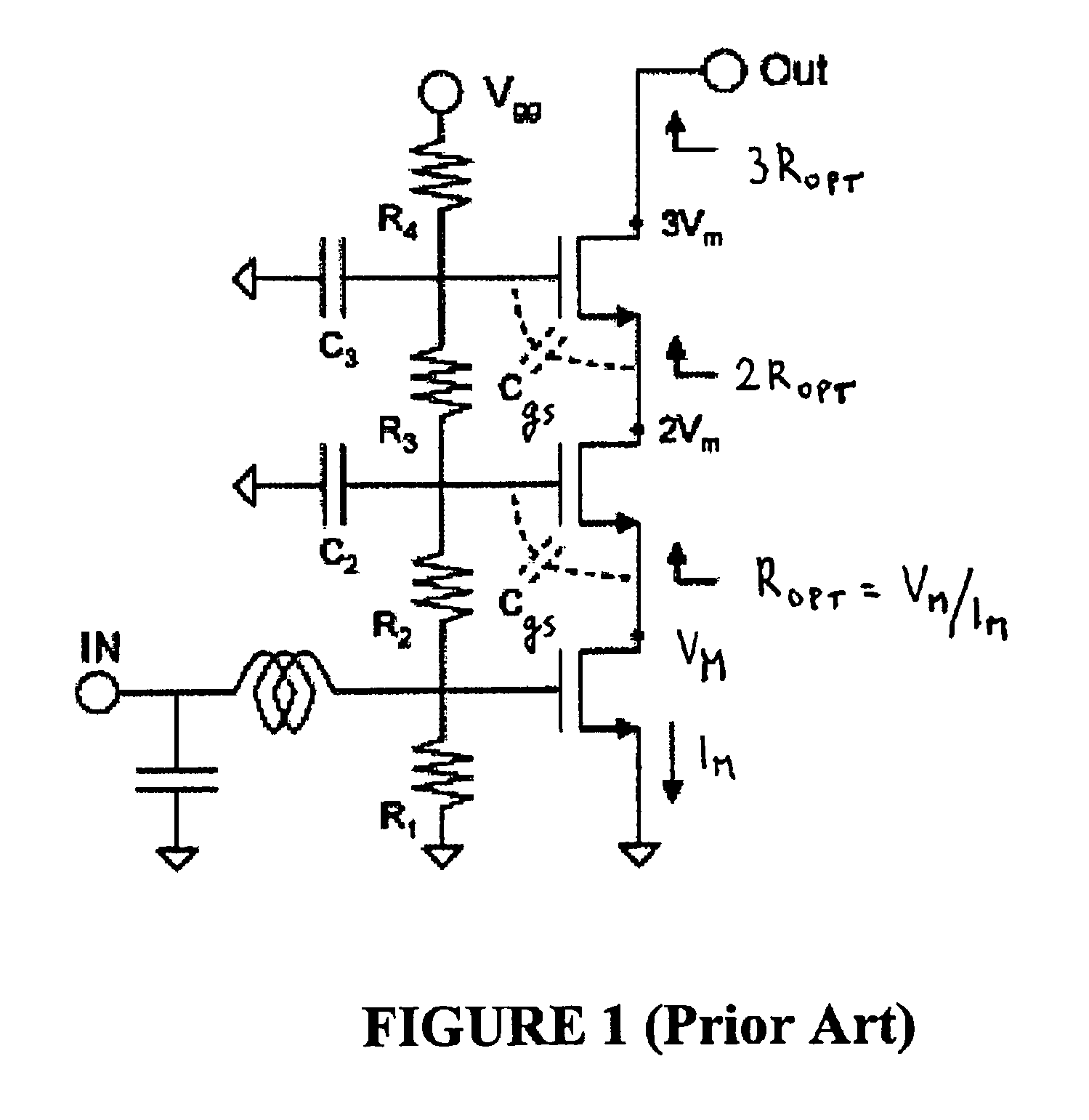
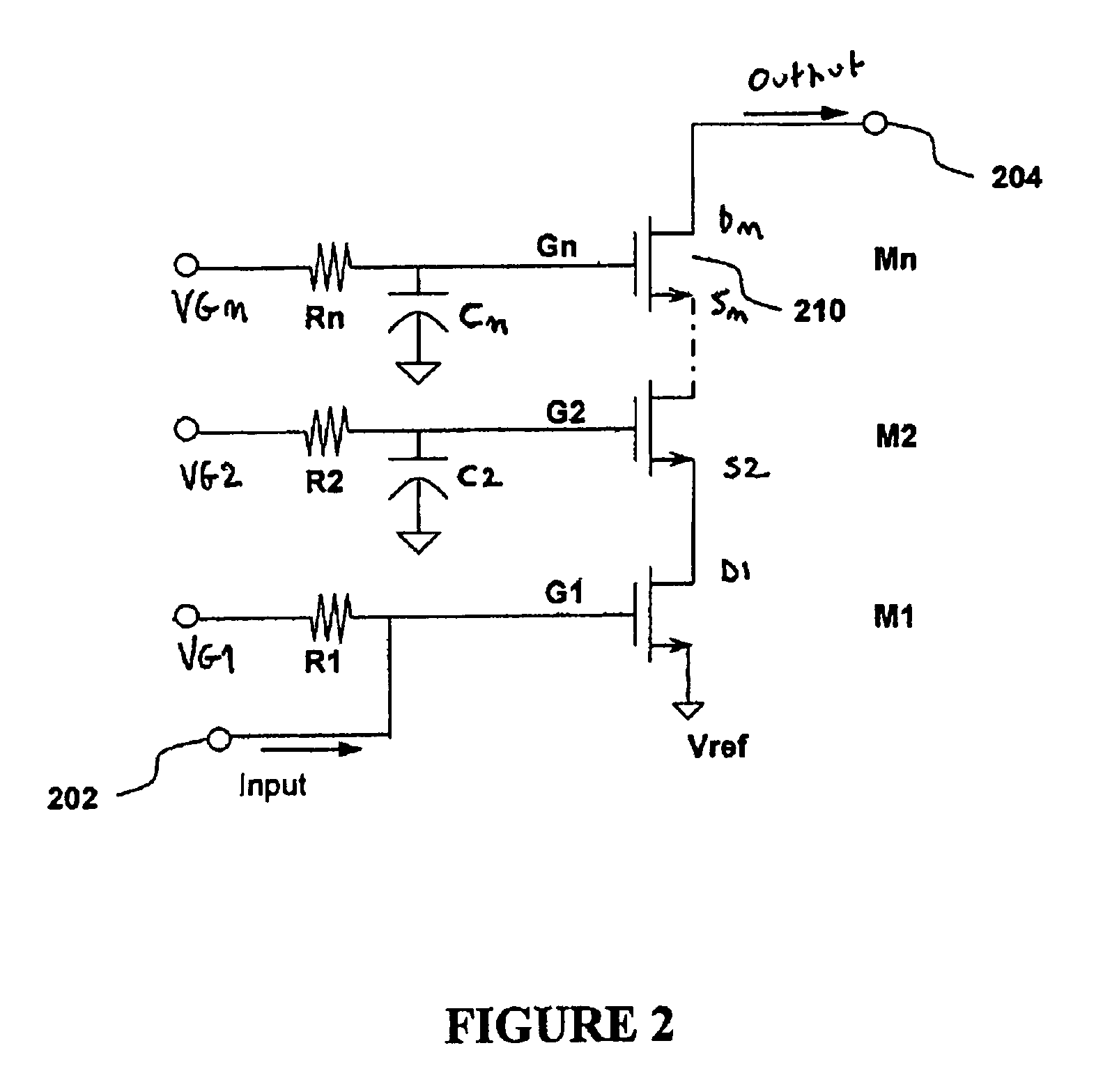
[0025]According to the present teachings, a serially-connected PA is provided, comprising several transistors stacked one above the other, forming an input stage and one or more additional stages stacked above the input stage, wherein: 1) the input voltage bias of the input stage and the one or more additional stages; and 2) the external gate capacitances of the one or more additional stages are configured to reduce distortion among stages. According to this embodiment, configuration of the input voltage bias of the input stage and additional stages allows minimization of the generation of non-linearities from each device. On the other hand, configuration of the external gate capacitances of the one or more additional stages allows phase alignment between devices to maximize cancellation of distortion between such devices. By way of example and not of limitation, reduction of distortion among stages can be performed by minimizing intermodulation distortion (IMD) of the PA In particu...

case 1

[0087) This is a scenario wherein the input power is small so that the product between

[0088]50⁢vgs⁢⁢1123

and the fifth order coefficients is far smaller than the third order coefficients:

[0089]Hence, the equations (18) and (19) set forth above become:

[0090]RA⁢⁢1+p⁢gm⁢⁢12gm⁢⁢11⁢RA⁢⁢2=0(Eq.⁢21)IA⁢⁢1+p⁢gm⁢⁢12gm⁢⁢11⁢IA⁢⁢2=0(Eq.⁢22)

[0091]In this scenario, even without the second column, it is also possible to tune the bias points VG11, VG21 in order to obtain the desired result of RA1=0, IA1=0. However, this is a problem of three unknowns for three independent equations. The optimal bias points should be one or few discrete points. In a real power amplifier, process, voltage and temperature (PVT) variation will get the bias away from optimal points. PVT sensing and bias adjustment can improve such disadvantage, but are limited by sensing sensitivity and accuracy.

[0092]On the other hand, if the parallel array of FIG. 6 is used, there are six unknowns to meet four independent equations (20)...

case 2

[0093) This is a scenario wherein the input power has a value such that the product of

[0094]50⁢vgs⁢⁢1123

with the fifth order coefficients is negligible with respect to the third order coefficients.

[0095]To minimize the IM3R, equations (18) and (19) become:

[0096]RB⁢⁢1+p⁢gm⁢⁢12gm⁢⁢11⁢RB⁢⁢2=0(Eq.⁢23)IB⁢⁢1+p⁢gm⁢⁢12gm⁢⁢11⁢IB⁢⁢2=0(Eq.⁢24)RA⁢⁢1+p⁢gm⁢⁢12gm⁢⁢11⁢RA⁢⁢2=0(Eq.⁢25)IA⁢⁢1+p⁢gm⁢⁢12gm⁢⁢11⁢IA⁢⁢2=0(Eq.⁢26)

[0097]In this scenario, there are six unknowns to meet six independent equations (20), (23), (24), (25) and (26). The parallel array of FIG. 6 can cancel distortion totally, but the bias may be sensitive to PVT variations. As described above with reference to case 1, PVT sensing and bias adjustment can provide improvement, but as described above, are limited by sensing sensitivity and accuracy.

[0098]If there is only one column, it would be impossible in this second case to cancel distortion over the entire input level.


PUM


Abstract

A power amplifier with stacked, serially connected, field effect transistors is described. DC control voltage inputs are fed to the gates of each transistor. Capacitors are coupled to the transistors. The inputs and the capacitors are controlled to minimize generation of non-linearities of each field effect transistor and / or to maximize cancellation of distortions between the field effect transistors of the power amplifier in order to improve linearity of the power amplifier output.

Description

BACKGROUND[0001]1. Field[0002]The present teachings relate to reduction of distortion in electrical circuits. More particularly, the present teachings relate to a stacked linear power amplifier having capacitor feedback and resistor isolation.[0003]2. Description of Related Art[0004]Power amplifiers (PA) convert low-power signals into signals having a larger power. The prior art is replete with different PA designs and techniques for amplifying power. For example, J. Jeong, S. Pornpromlikit, P. M. Asbeck, D. Kelly, “A 20 dBm Linear RF Power Amplifier Using Stacked Silicon-on-Sapphire MOSFETs, IEEE Microwave and Wireless Components Letters, Vol. 16, No. 12, December 2006, discloses a serially-connected power amplifier (PA). See FIG. 1 of the present application, wherein a triple-stacked FET PA is shown. Jeong is concerned with obtaining large voltage swings at the gate of each FET and does so by providing the two top FETs with a capacitive voltage divider comprising the gate-to-sourc...

Claims


Application Information

Patent Timeline
Patent Type & Authority Patents(United States)
IPC IPC(8): H03F3/04
CPCH03F1/223H03F1/342H03F3/423H03F2200/18
Inventor LI, YANG EDWARDBROUGHTON, ROBERTBACON, PETERBONKOWSKI, JAMES
Owner PSEMI CORP
Why Eureka
Try Eureka