Electronic device, light-receiving and light-emitting device, electronic integrated circuit and optical integrated circuit using the devices

a technology of electronic components and integrated circuits, applied in the direction of basic electric elements, semiconductor devices, electrical equipment, etc., can solve the problems that the graphene sheet is not applicable to electronic devices such as transistors or light, and the method of controlling the band gap using microfabrication technology has not been found

Inactive Publication Date: 2013-08-13
HITACHI LTD
View PDF22 Cites 3 Cited by
  • Summary
  • Abstract
  • Description
  • Claims
  • Application Information

AI Technical Summary

Benefits of technology

[0018]According to the present invention, the electron configuration of a graphene sheet can be controlled by microfabrication technologies and the band gap thereof can be controlled.

Problems solved by technology

Therefore, the graphene sheet is not applicable for electronic devices such as transistors or light-receiving and light-emitting devices such as LEDs.
However, methods for controlling the band gap using microfabrication technologies have not been found.

Method used


Image

  • Electronic device, light-receiving and light-emitting device, electronic integrated circuit and optical integrated circuit using the devices
  • Electronic device, light-receiving and light-emitting device, electronic integrated circuit and optical integrated circuit using the devices
  • Electronic device, light-receiving and light-emitting device, electronic integrated circuit and optical integrated circuit using the devices

Examples


embodiment 1

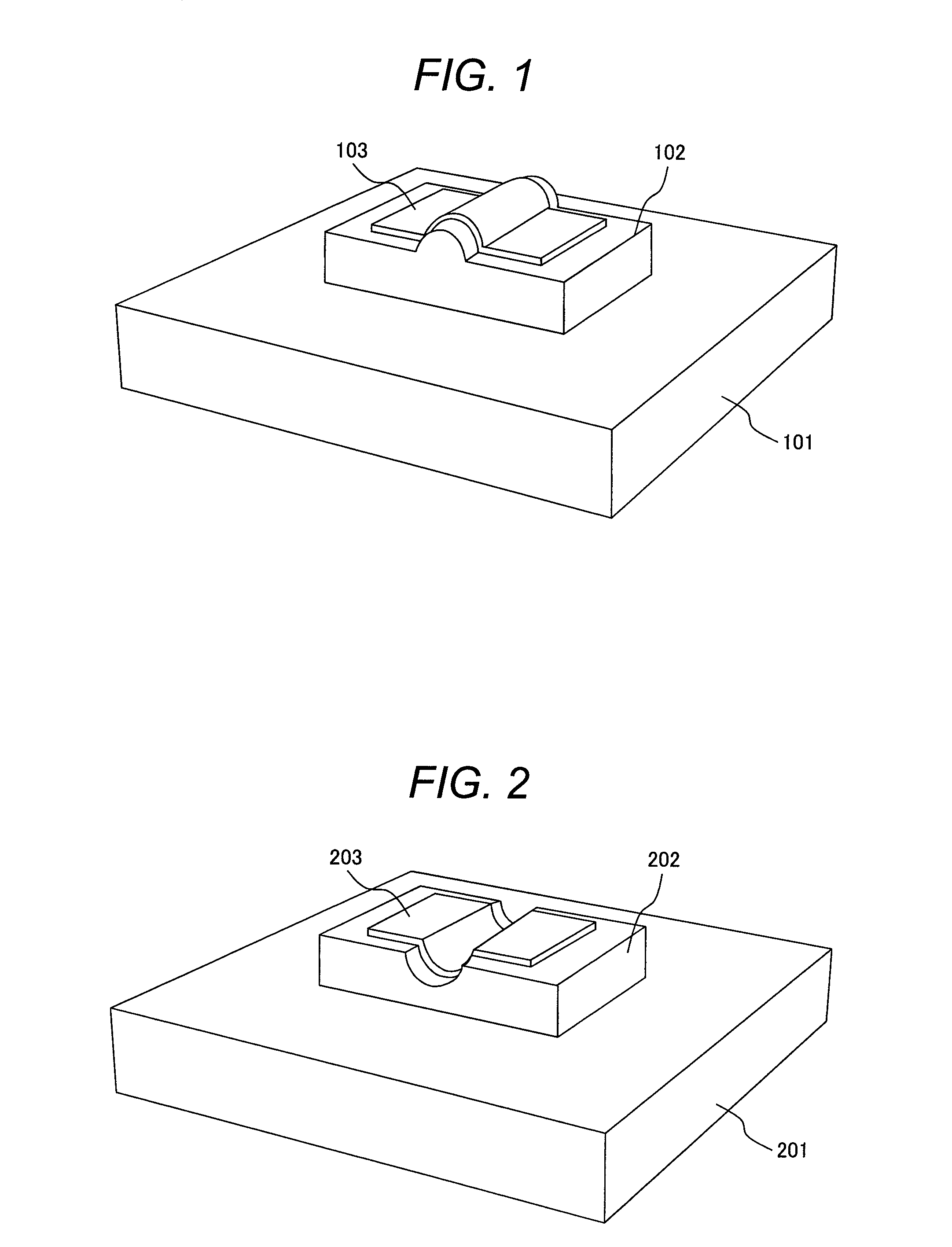
[0028]Embodiment 1 will be described with reference to FIG. 1. FIG. 1 is a schematic view showing one embodiment in which a graphene sheet is disposed along a semi-cylindrical convex structure of a base layer.

[0029]A vapor-phase growth method, a photolithography process and a dry etching process are performed in this sequence on the surface of a substrate 101 (a Si substrate) to form a base layer 102 having a semi-cylindrical convex structure. The base layer 102 has a thickness of 10 nm and a material thereof is aluminium oxide. The semi-cylindrical structure has a diameter of 3 nm, a length in a transverse direction of 30 nm and a depth of 30 nm.

[0030]Then, graphene is selectively grown only on the surface of the base layer 102 by a vapor-phase growth method using acetylene as a raw material gas. A growth temperature of the vapor-phase growth is 400° C. and a growth time thereof is ten minutes. The graphene is not grown on the substrate 101, but selectively grown only on the alumin...

embodiment 2

[0035]Embodiment 2 will be described with reference to FIG. 2.

[0036]Embodiment 2 is different from embodiment 1 in that a graphene layer 203 is formed on a base layer 202 after forming the base layer 202 having a semi-cylindrical concave structure. A method for forming the semi-cylindrical concave structure of the base layer 202 and a method for forming the graphene layer 203 are similar to the methods described in embodiment 1.
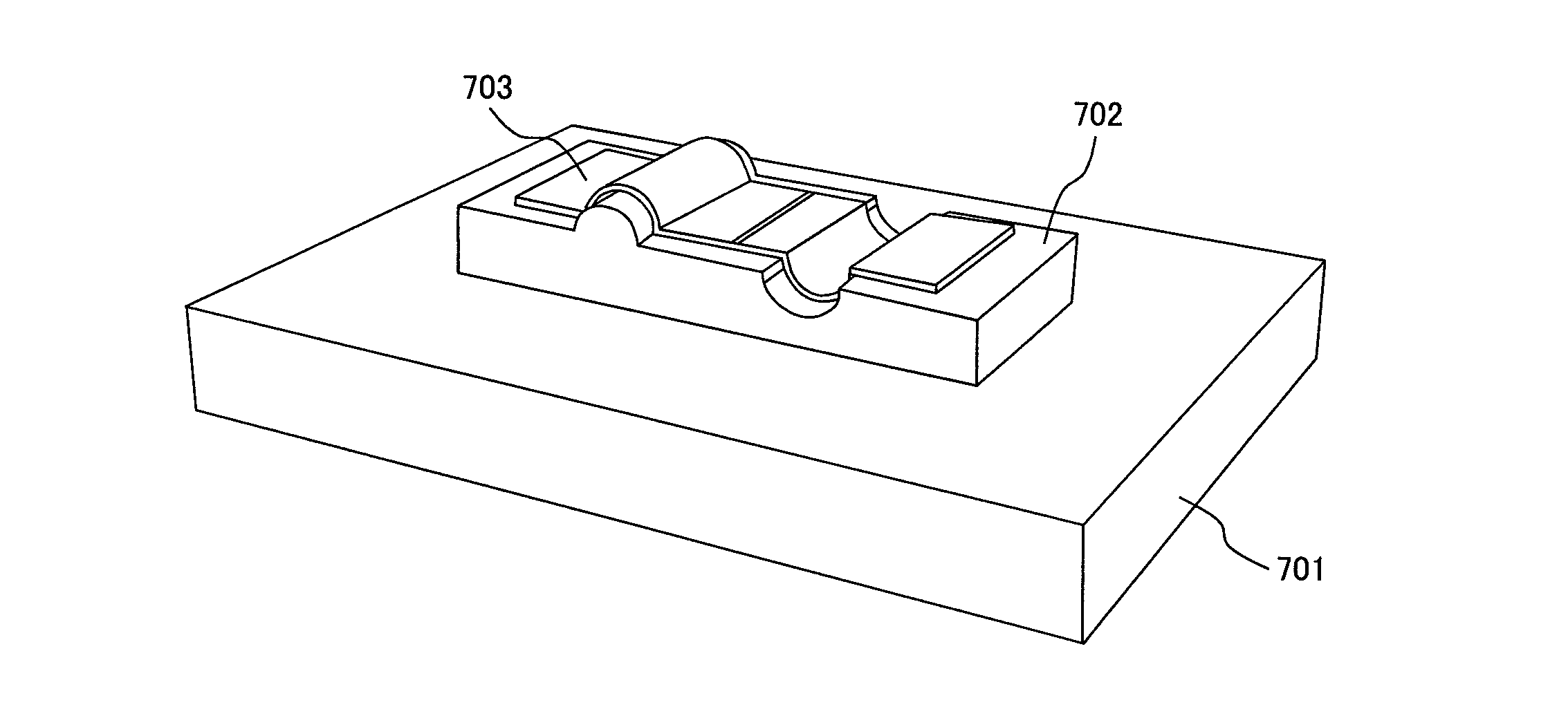
embodiment 3

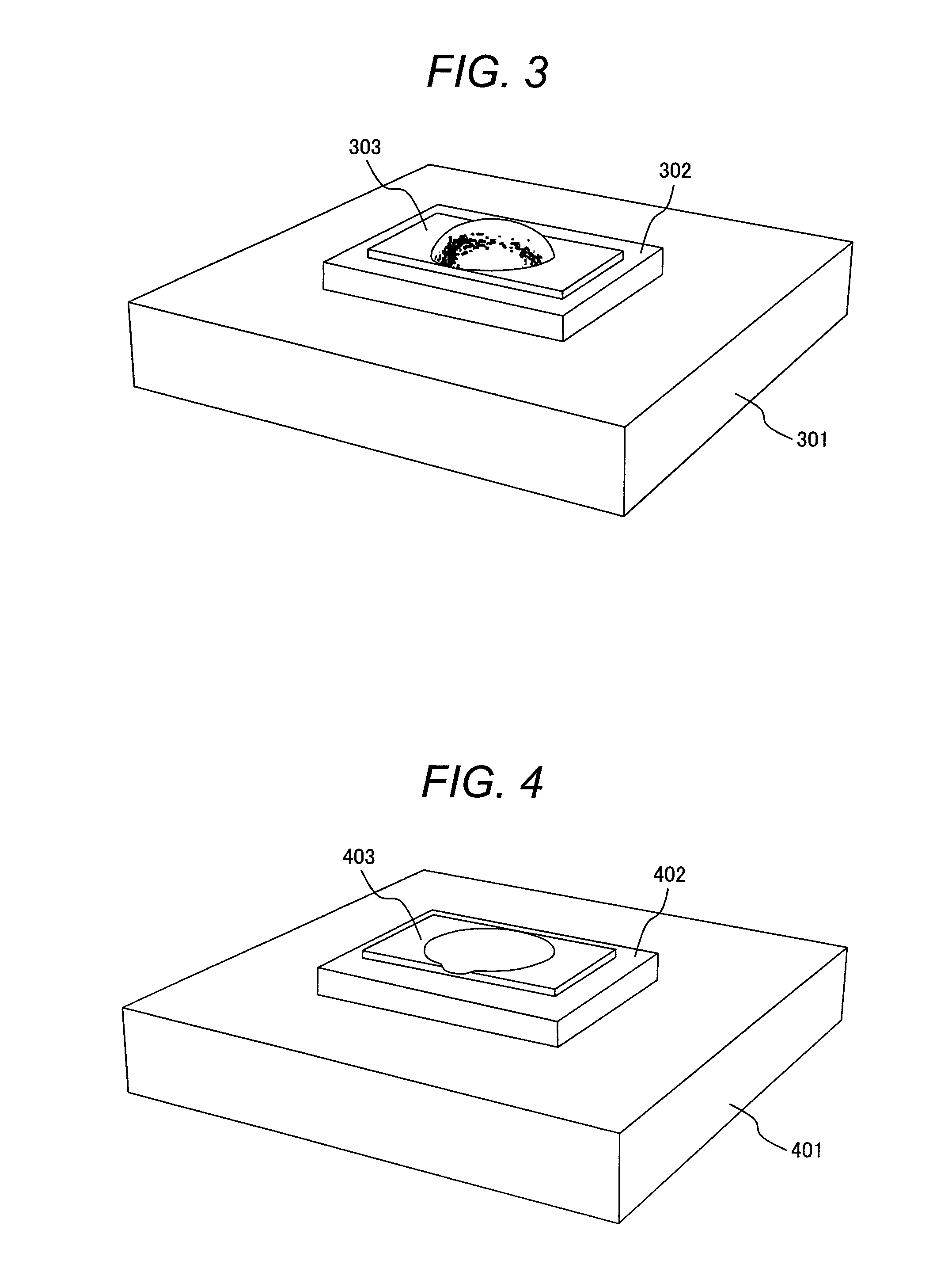
[0037]Embodiment 3 will be described with reference to FIG. 3.

[0038]Embodiment 3 is different from embodiment 1 in that a graphene layer 303 is formed on a base layer 302 after forming the base layer 302 having a hemispherical convex structure. A method for forming the hemispherical convex structure of the base layer 302 and a method for forming the graphene layer 303 are similar to the methods described in embodiment 1.


PUM


Abstract

Provided are an electronic device and a light-receiving and light-emitting device which can control the electron configuration of a graphene sheet and the band gap thereof, and an electronic integrated circuit and an optical integrated circuit which use the devices. By shaping the graphene sheet into a curve, the electron configuration thereof is controlled. The graphene sheet can be shaped into a curve by forming the sheet on a base film having a convex structure or a concave structure. The local electron states in the curved part can be formed by bending the graphene sheet. Thus, the same electron states as the cylinder or cap part of a nanotube can be realized, and the band gaps at the K points in the reciprocal lattice space can be formed.

Description

TECHNICAL FIELD[0001]The present invention relates to an electronic device and a light-receiving and light-emitting device having a graphene sheet, and an electronic integrated circuit and an optical integrated circuit which use the devices.BACKGROUND ART[0002]A two-dimensional structure in which carbon atoms are regularly arranged in hexagon configuration is called a graphene sheet. A substance formed by stacking a plurality of the graphene sheets is called graphite. The graphene sheet and the graphite have been known. A single sheet of graphene sheet can have been taken out onto a substrate recently (for example, see Non patent document 1), so that the graphene sheet has suddenly attracted attention.[0003]A graphene sheet shows metallic properties because a π band and a π* band contact at the K points in the reciprocal lattice space. Therefore, the graphene sheet is not applicable for electronic devices such as transistors or light-receiving and light-emitting devices such as LEDs...

Claims


Application Information

Patent Timeline
Patent Type & Authority Patents(United States)
IPC IPC(8): H01L29/06H01L29/78
CPCH01L29/1606H01L29/7781H01L29/7843H01L29/78684H01L29/78696H01L51/0558H01L21/02381H01L21/02488H01L21/02527H01L33/0041H01L33/40H10K10/484
Inventor OKAI, MAKOTO
Owner HITACHI LTD
Why Eureka
Try Eureka