

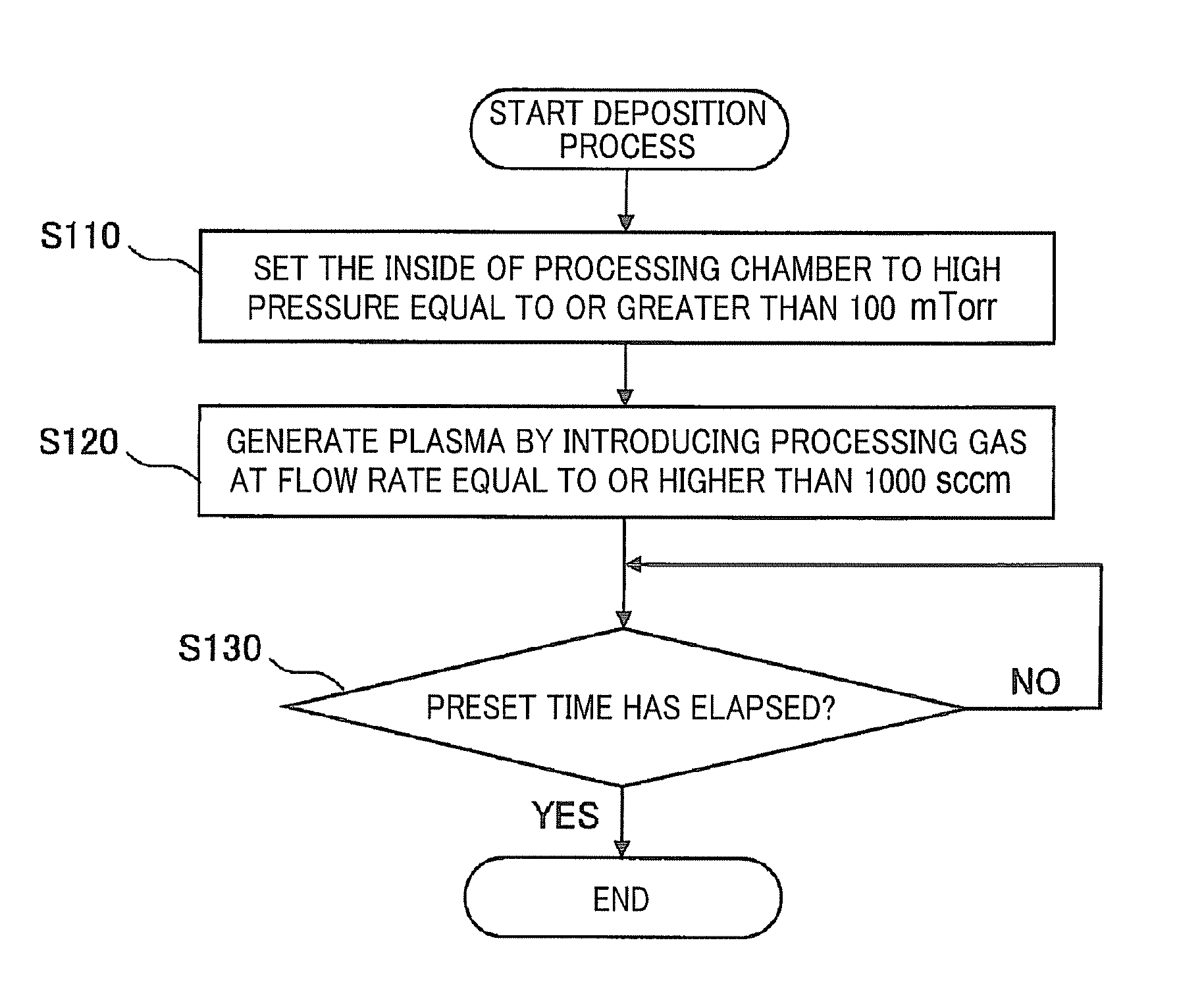
Substrate processing method
a processing method and substrate technology, applied in the direction of superimposed coating process, resistive material coating, liquid/solution decomposition chemical coating, etc., can solve the problem of non-uniform critical dimension (cd) of patterns formed after etching, failure to obtain design device characteristics, and critical dimension deviation of pattern formation after etching observed to become non-uniform, etc. problem, to achieve the effect of increasing the internal pressure of the processing chamber, reducing the degree of uniformity of deposition degree degree degr
- Summary
- Abstract
- Description
- Claims
- Application Information
AI Technical Summary
Benefits of technology
Problems solved by technology
Method used
Image

Examples
Embodiment Construction
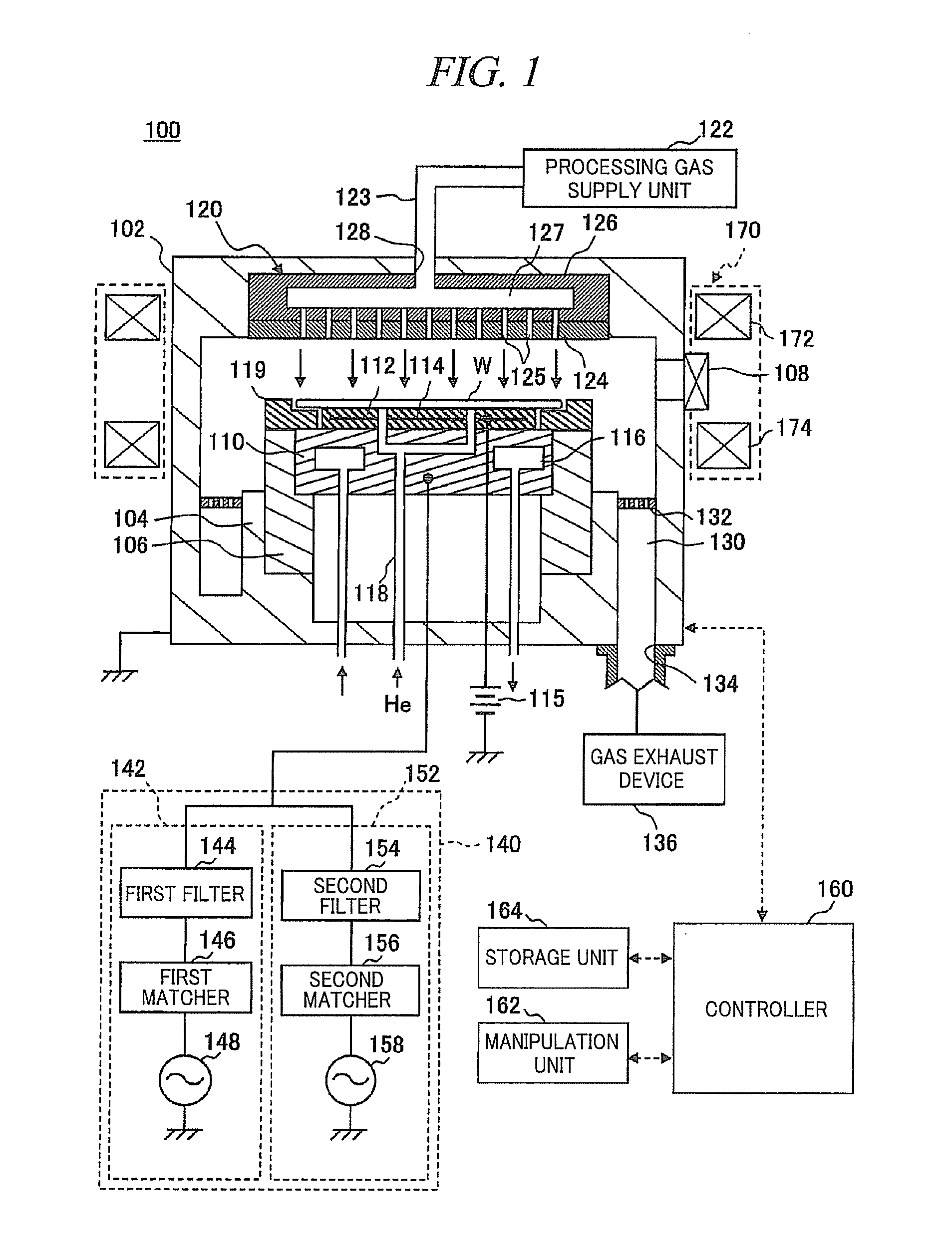
[0039]Hereinafter, embodiments of the present disclosure will be explained in detail with reference to accompanying drawings. Through the present specification and drawings, parts having substantially same function and configuration will be assigned same reference numerals, and redundant description will be omitted.
[0040](Configuration Example of a Substrate Processing Apparatus)
[0041]Above all, a configuration example of a substrate processing apparatus in accordance with an embodiment of the present disclosure will be explained with reference to the drawings. Herein, there will be explained a substrate processing apparatus configured as a plasma processing apparatus in which an etching target film on a wafer W is etched by applying a first high frequency power (high frequency power for plasma generation) of a relatively high frequency of, e.g., about 40 MHz and a second high frequency power (high frequency power for a bias voltage) of a relatively low frequency of, e.g., about 13....
PUM
| Property | Measurement | Unit |
|---|---|---|
| pressure | aaaaa | aaaaa |
| pressure | aaaaa | aaaaa |
| residence time | aaaaa | aaaaa |
Abstract
Description
Claims
Application Information