Purification of metal nanostructures for improved haze in transparent conductors made from the same
a technology of transparent conductors and metal nanostructures, which is applied in the direction of electrically-conductive paints, conductive layers on insulating supports, transportation and packaging, etc., can solve the problems of not all of the nanostructures desirable, and the morphologies of the nanostructure are not good
- Summary
- Abstract
- Description
- Claims
- Application Information
AI Technical Summary
Benefits of technology
Problems solved by technology
Method used
Image
Examples
example 1
Purification by Acetone Wash
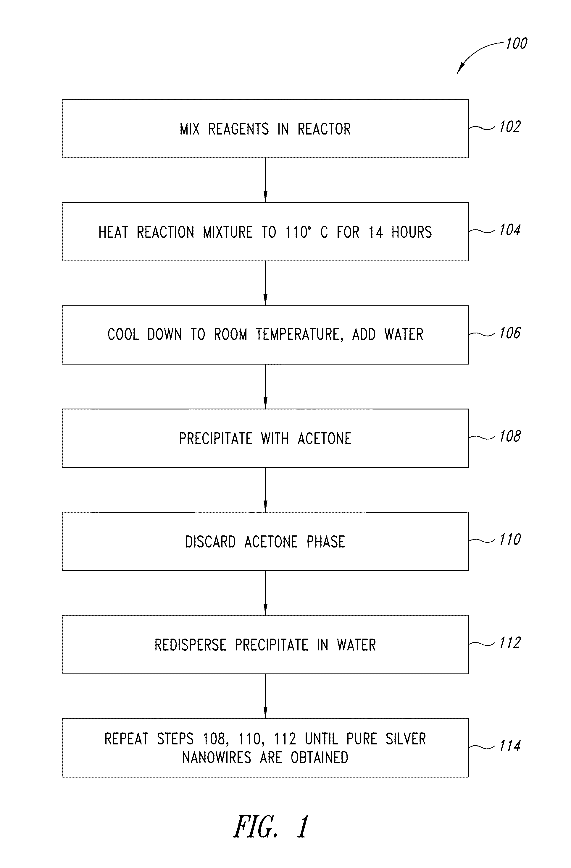
[0081]To 500 g of glycerol in a clean glass bottle was added 7.5 g PVP, 55 mg TBAC, 2.5 g silver nitrate. The bottle was capped and the mixture was heated in a 110° C. convection oven for about 14 hours. Once the reaction mixture was cooled to 30° C., 500 g of DIW was added. The crude diluted reaction mixture was added to 2 kg of acetone, producing a semi-solid dark brown precipitate. The supernatant liquid was separated from the semi-solid precipitate by decantation or by filtration through a medium porosity glass frit. Unexpectedly, the silver nanowires contained in this precipitate could easily be re-suspended in DIW. Thus, the precipitate was then re-suspended in about 200 g DIW and re-precipitated in 800 g acetone. These precipitation / re-suspension steps were repeated several times until a light tan fluffy precipitate was obtained. This precipitate was re-suspended in DIW and was found to contain mainly thin and long silver nanowires, almost free of ...
example 2
Transparent Conductors Made of Purified Nanowires
[0082]Transparent conductive thin films were prepared by spin coating, on a glass substrate, an ink composition comprising the purified silver nanowires of Example 1 and HPMC in water. Comparative samples of transparent conductors were also similarly prepared using silver nanowires that were similarly synthesized except for the respective polyol solvents used in each synthesis and the post-synthesis acetone wash. Table 1 demonstrates that, for a given sheet resistivity, the transmission and haze are considerably improved in the transparent conductor formed of the purified silver nanowires obtained from the glycerol solvent, because of a reduced number of low aspect ratio nanostructures as well as the thinner diameters in the nanowires.
[0083]
TABLE 1No Acetone WashAcetone WashPolyol solventEthylene glycolGlycerol% Transmission88.190.1% Haze2.851.54Resistivity2524
example 3
Counts of Bright Objects in Transparent Conductive Film
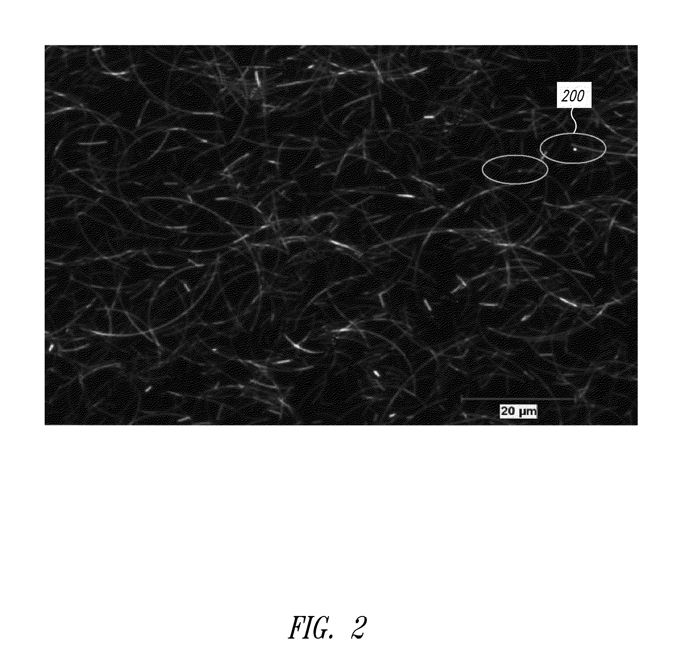
[0084]Conductive film was prepared by spin coating as described in Example 2. The number of the low aspect ratio nanostructures was determined by visualizing a conductive film formed of purified silver nanowires under a microscope at approximately 100× magnification and in dark field mode. Pictures were taken of multiple frames and the low aspect ratio nanostructures counted (FIG. 2). The low aspect ratio nanostructures 200 were typically brighter, shorter or wider than the silver nanowires. In particular, the low aspect ratio nanowires had an aspect ratio of less than 10. The counts of each frame were averaged and converted to per unit surface area.
[0085]Table 2 shows the counts of the low aspect ratio nanostructures in two films of different loading densities, which correspond to respective resistances, transmission, and haze. In particular, the haze of film 2 is 50% of that of Film 1 because of, at least in part, a fewer numb...
PUM
| Property | Measurement | Unit |
|---|---|---|
| haze | aaaaa | aaaaa |
| aspect ratio | aaaaa | aaaaa |
| haze | aaaaa | aaaaa |
Abstract
Description
Claims
Application Information

