Backside illuminated sensor and manufacturing method thereof

a technology of backside illumination and image sensor, which is applied in the direction of semiconductor devices, semiconductor/solid-state device details, radiation control devices, etc., can solve the problems of image loss, increased noise, and reduced light received in one light receiving element, so as to improve light receiving efficiency and minimize light into the light receiving element. , the effect of easy control of the back grinding process

Active Publication Date: 2013-10-22
SK HYNIX INC
View PDF34 Cites 13 Cited by
  • Summary
  • Abstract
  • Description
  • Claims
  • Application Information

AI Technical Summary

Benefits of technology

[0007]According to the present invention as described above, the following effects can be achieved.
[0008]First, the backside illuminated image sensor can receive light from the backside of a wafer (substrate), so that the loss of light into the light receiving element can be minimized, thereby improving light receiving efficiency, as compared with a conventional CMOS image sensor (a front-side illuminated image sensor).
[0009]Second, according to the method for manufacturing the backside illuminated image sensor using the back grinding process of the present invention, the alignment key having a via hole shape is formed in the substrate before the back grinding process for the backside of the substrate, and the backside grinding target of the substrate is controlled using the alignment key during the back grinding process, so that the back grinding process can be easily controlled.
[0010]Third, the front side of the alignment key is connected to the interconnection layer formed on the front side of the substrate, and the backside of the alignment key is exposed to the backside of the substrate and connected to the pad. Thus, the alignment key is used as a contact plug connecting the pad to the interconnection layer, so that the pad can be arranged on the backside of the substrate, other than the front side of the substrate. Consequently, various designs are possible in the packaging process.
[0011]Fourth, according to the present invention, the spacer is formed on the inner sidewall of the via hole, thereby preventing a leakage current from flowing from the conductive alignment key connecting the pad to the interconnection layer to the first substrate.
[0012]Fifth, according to the present invention, the spacer having high etching selectivity relative to the first substrate is formed on the inner sidewall of the via hole, so that a process margin can be ensured during a subsequent process of etching the backside of the first substrate and the alignment key can be prevented from being damaged by etchant during the etching process.

Problems solved by technology

Therefore, the amount of light received in one light receiving element is reduced, causing various problems such as image loss resulting from an increase in noise.

Method used


Image

  • Backside illuminated sensor and manufacturing method thereof
  • Backside illuminated sensor and manufacturing method thereof
  • Backside illuminated sensor and manufacturing method thereof

Examples


Embodiment Construction

Technical Problem

[0004]Accordingly, the present invention has been made to solve the above-mentioned problems occurring in the prior art, and the present invention provides a backside illuminated image sensor, in which light is illuminated from the backside of a wafer, and a method for manufacturing the same.

Technical Solution

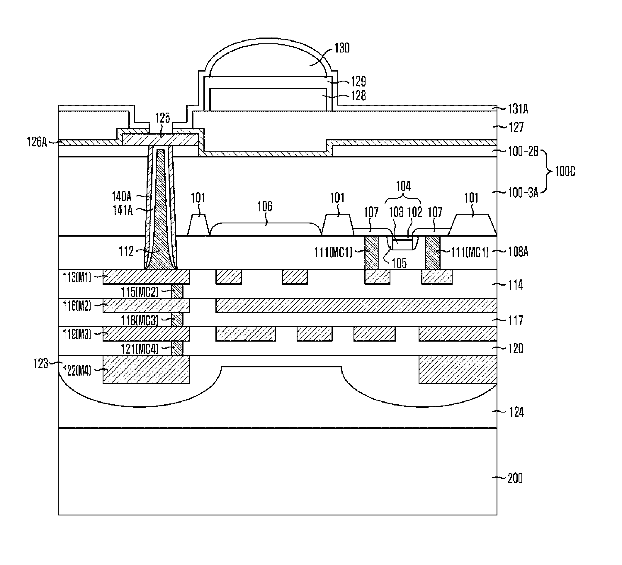
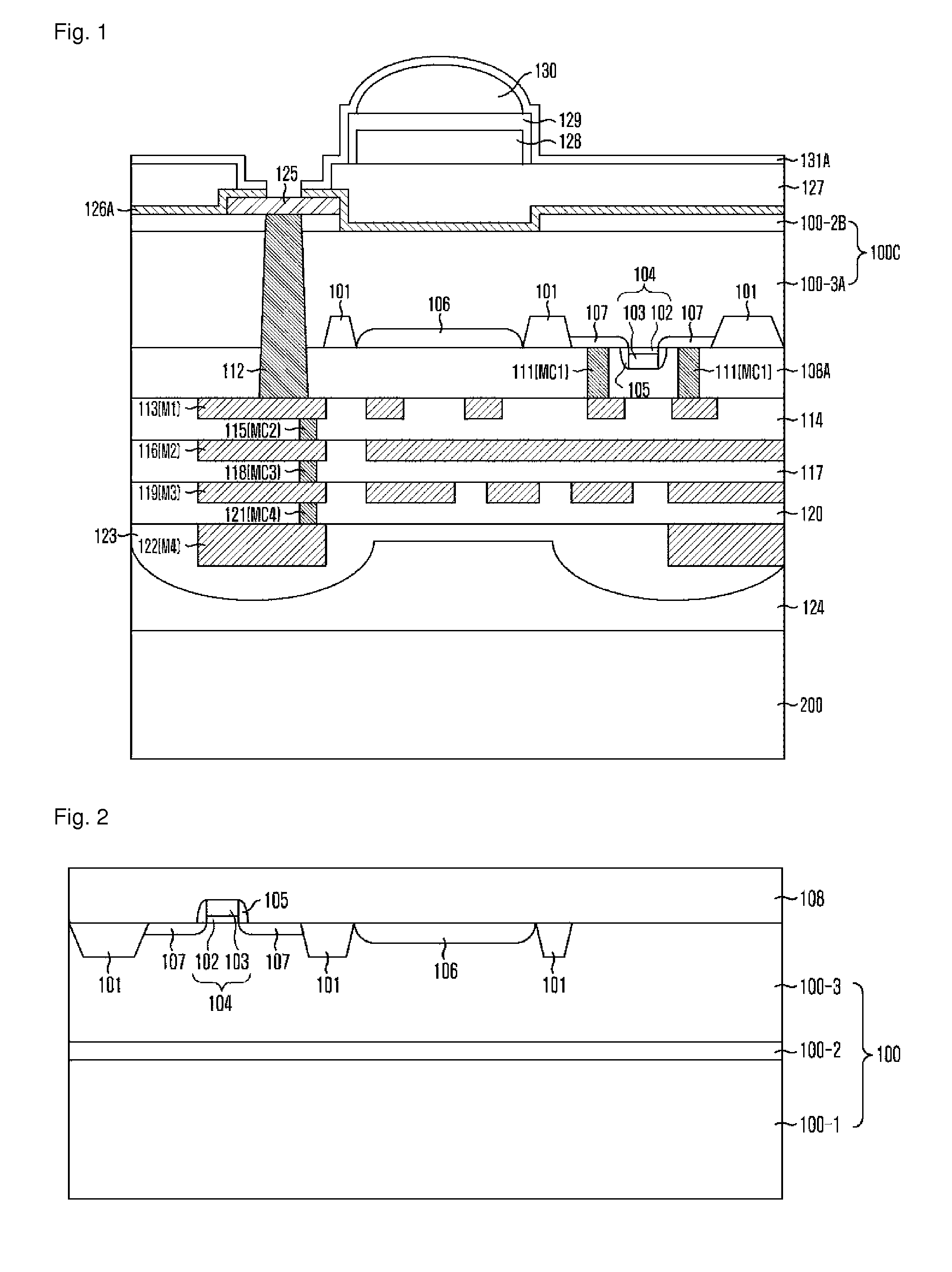
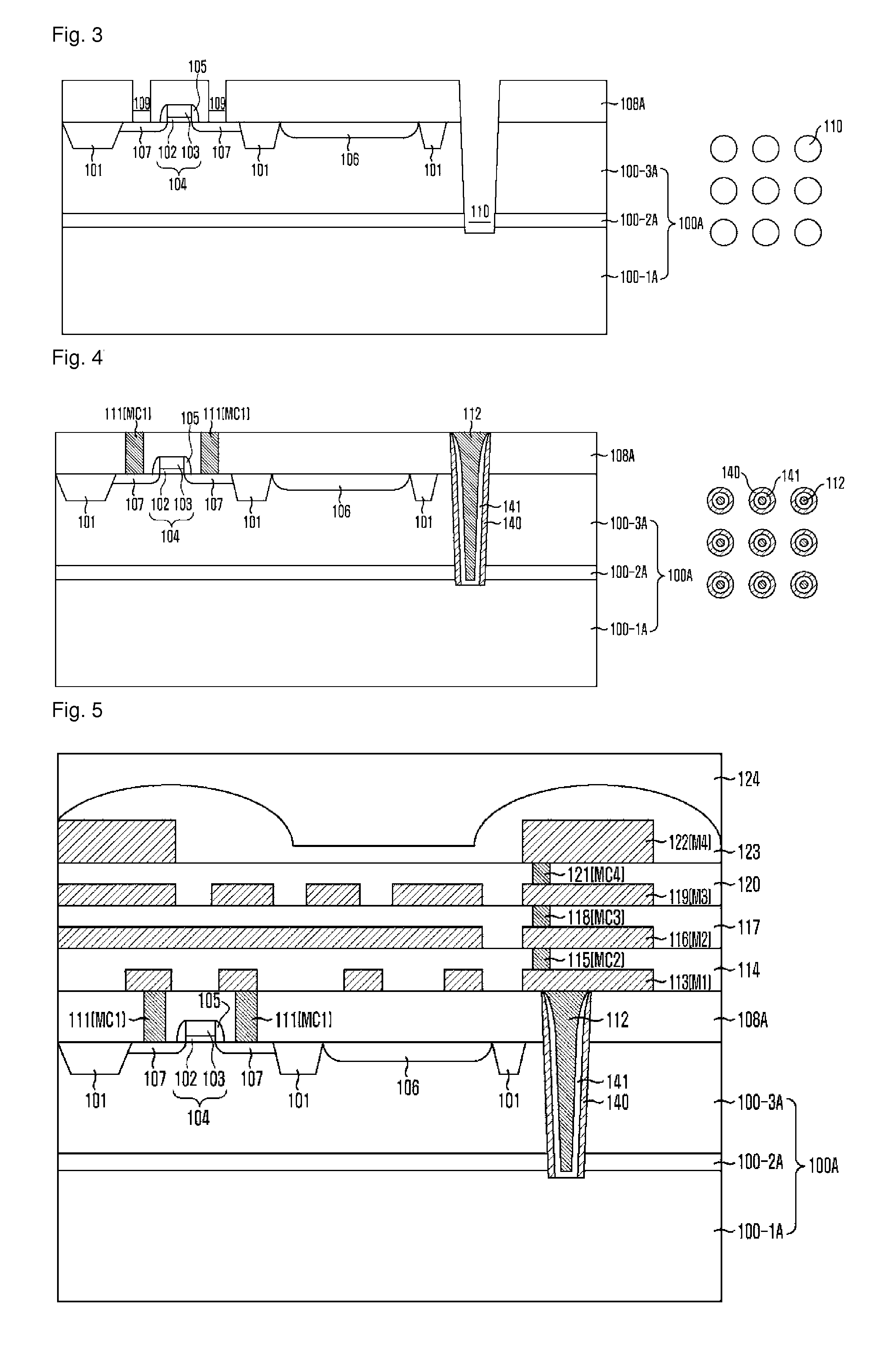
[0005]In accordance with an aspect of the present invention, there is provided a backside illuminated image sensor including a light receiving element formed in a first substrate, an interlayer insulation layer formed on the first substrate including the light receiving element, a via hole formed through the interlayer insulation layer and the first substrate while being spaced apart from the light receiving element, a spacer formed on an inner sidewall of the via hole, an alignment key to fill the via hole, interconnection layers formed on the interlayer insulation layer in a multilayer structure in which a backside of a lowermost layer of the interconnection ...


PUM


Abstract

Disclosed is a backside illuminated image sensor including a light receiving element formed in a first substrate, an interlayer insulation layer formed on the first substrate including the light receiving element, a via hole formed through the interlayer insulation layer and the first substrate while being spaced apart from the light receiving element, a spacer formed on an inner sidewall of the via hole, an alignment key to fill the via hole, interconnection layers formed on the interlayer insulation layer in a multilayer structure in which a backside of a lowermost layer of the interconnection layers is connected to the alignment key, a passivation layer covering the interconnection layers, a pad locally formed on a backside of the first substrate and connected to a backside of the alignment key, and a color filter and a microlens formed on the backside of the first substrate corresponding to the light receiving element.

Description

CROSS-REFERENCE TO RELATED APPLICATIONS[0001]The present application is a 35 U.S.C. §371 national stage filing of PCT Application PCT / KR2009 / 003113, filed Jun. 10, 2009, which claims priority to KR Application 10-2008-0054876, filed Jun. 11, 2008. Each of the above-identified applications are incorporated herein by reference in their entirety.TECHNICAL FIELD[0002]The present invention relates to a semiconductor manufacturing technology, particularly to an image sensor and a method for manufacturing the same, and more particularly to a backside illuminated image sensor and a method for manufacturing the same.BACKGROUND ART[0003]In a general complementary metal oxide semiconductor (CMOS) image sensor, a peripheral circuits such as a light receiving element unit, a digital control block and an analog-to-digital converter are arranged in a limited area within a chip. Thus, an area ratio of a pixel array per a chip area is limited to about 40%. Furthermore, a pixel size is reduced for th...

Claims


Application Information

Patent Timeline
Patent Type & Authority Patents(United States)
IPC IPC(8): H01L23/48
CPCH01L23/481H01L27/14632H01L27/14636H01L27/1464H01L27/1469H01L2924/0002H01L2924/00H01L27/146
Inventor PYO, SUNG-GYU
Owner SK HYNIX INC
Why Eureka
Try Eureka