Solid-state image sensor and method for producing the same

a solid-state image and sensor technology, applied in the field of solid-state image sensors, can solve the problems of short time in which the photodiode is exposed to light to obtain one frame of pixel signals, the portion of the charge cannot reach the floating diffusion within the predetermined short photoelectric conversion, and the time required for the photocharge produced by the photodiode to reach the floating region is shortened, and the detection sensitivity and the s/n ratio are improved.

Active Publication Date: 2013-10-29
TOHOKU UNIV +1
View PDF14 Cites 9 Cited by
  • Summary
  • Abstract
  • Description
  • Claims
  • Application Information

AI Technical Summary

Benefits of technology

[0018]In the solid-state image sensor according to the present invention, the floating region, such as a floating diffusion, is formed substantially at the center of the light-receiving surface of the photodiode. This design significantly reduces the maximum distance from a given point on the light-receiving surface to the floating region as compared to case where the floating region is formed at one end of the light-receiving surface of the photodiode, so that the time required for the photocharges produced by the photodiode to reach the floating region is shortened. Therefore, even if the photocharge storage time is limited or the light-receiving surface of the photodiode is enlarged, there will be only a small amount of charges that will be discarded before reaching the floating region, i.e. that cannot be reflected in the optical signal, whereby the detection sensitivity and the S / N ratio are improved.
[0019]In the case where the potential is changed from the circumferential portion to the central portion of the light-receiving surface, the inclined or step-like potential change due to the difference in the concentration and / or depth of an impurity helps the photocharges produced by the photodiode to move from the circumference to the center of the light-receiving surface. Therefore, the photocharges easily accumulate around the transfer transistor, and when the transfer transistor is on, they will be efficiently and promptly transferred to the floating region. Thus, even in the case where the light-receiving surface of the photocharge is large-sized and the photocharge storage time is short, the photocharges produced by the photodiode will be efficiently collected and eventually reflected in the signal, whereby the detection sensitivity and S / N ratio are improved, so that the images obtained by high-speed imaging will have better qualities.

Problems solved by technology

In such a high-speed imaging operation, the period of time in which the photodiodes are exposed to light to obtain one frame of pixel signals is extremely short as compared to the normal imaging operation.
However, increasing the size of the light-receiving surface of the photodiode causes the following problem.
In this structure, when the size of the light-receiving surface of the photodiode is increased, the photocharges produced by the photodiode PD requires a non-negligible length of time to reach the floating diffusion PD, and a portion of the charges cannot be able to reach the floating diffusion within the predetermined short photoelectric conversion time.
As a result, the photocharge usage efficiency will deteriorate, and the detection sensitivity will not be improved to the expected level even if the size of the light-receiving surface of the photodiode; rather, it will be a major cause of image-quality deterioration.Patent Document 1: Japanese Unexamined Patent Application Publication No. 2001-345441Non-Patent Document 1: Kondo et al., “Kousokudo Bideo Kamera HyperVision HPV-1 no Kaihatsu (Development of “HyperVision HPV-1” High-Speed Video Camera)”, Shimadzu Hyouron (Shimadzu Review), Shimadzu Hyouron Henshuu-bu, Sep. 30, 2005, Vol. 62, No. 1 / 2, pp.

Method used


Image

  • Solid-state image sensor and method for producing the same
  • Solid-state image sensor and method for producing the same
  • Solid-state image sensor and method for producing the same

Examples


Embodiment Construction

[0064]A solid-state image sensor, which is an embodiment of the present invention, and a method for producing this image sensor are hereinafter described with reference to the attached drawings.

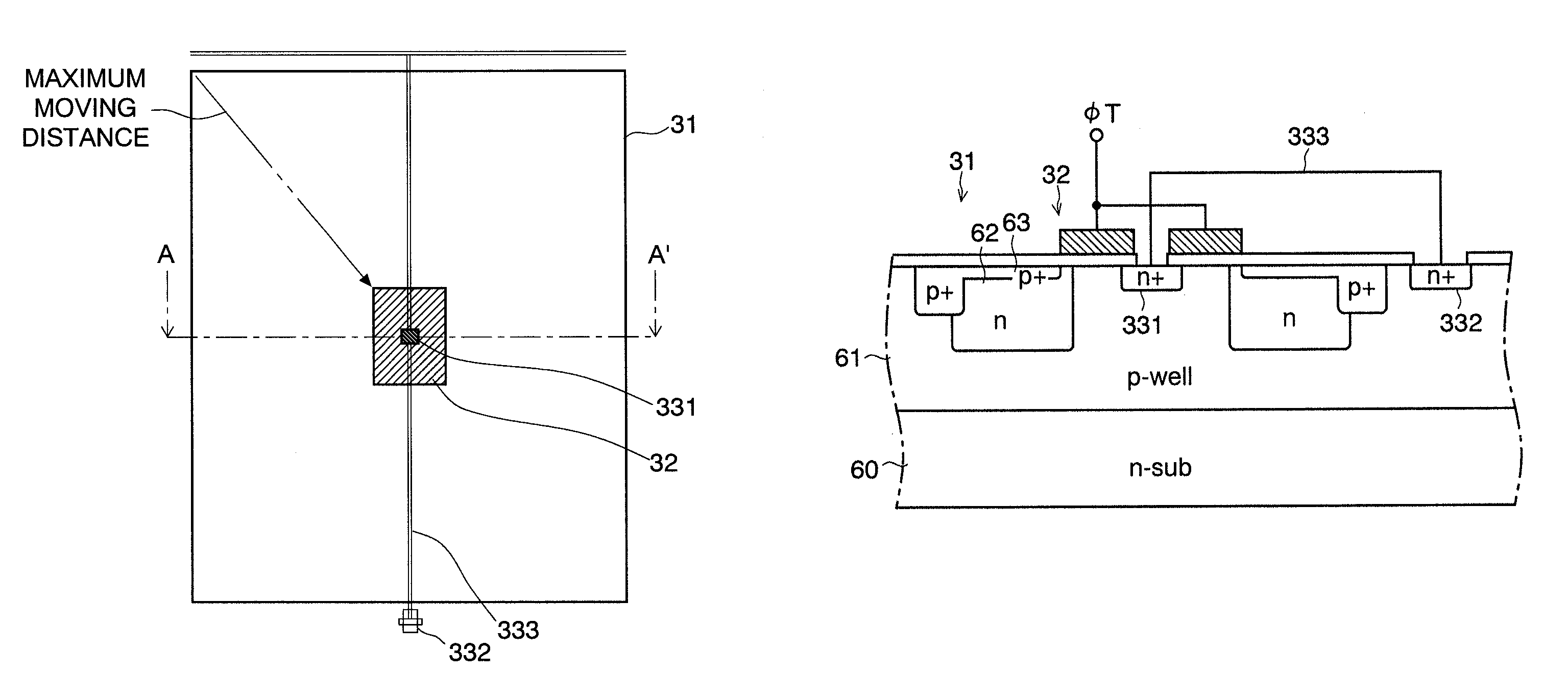
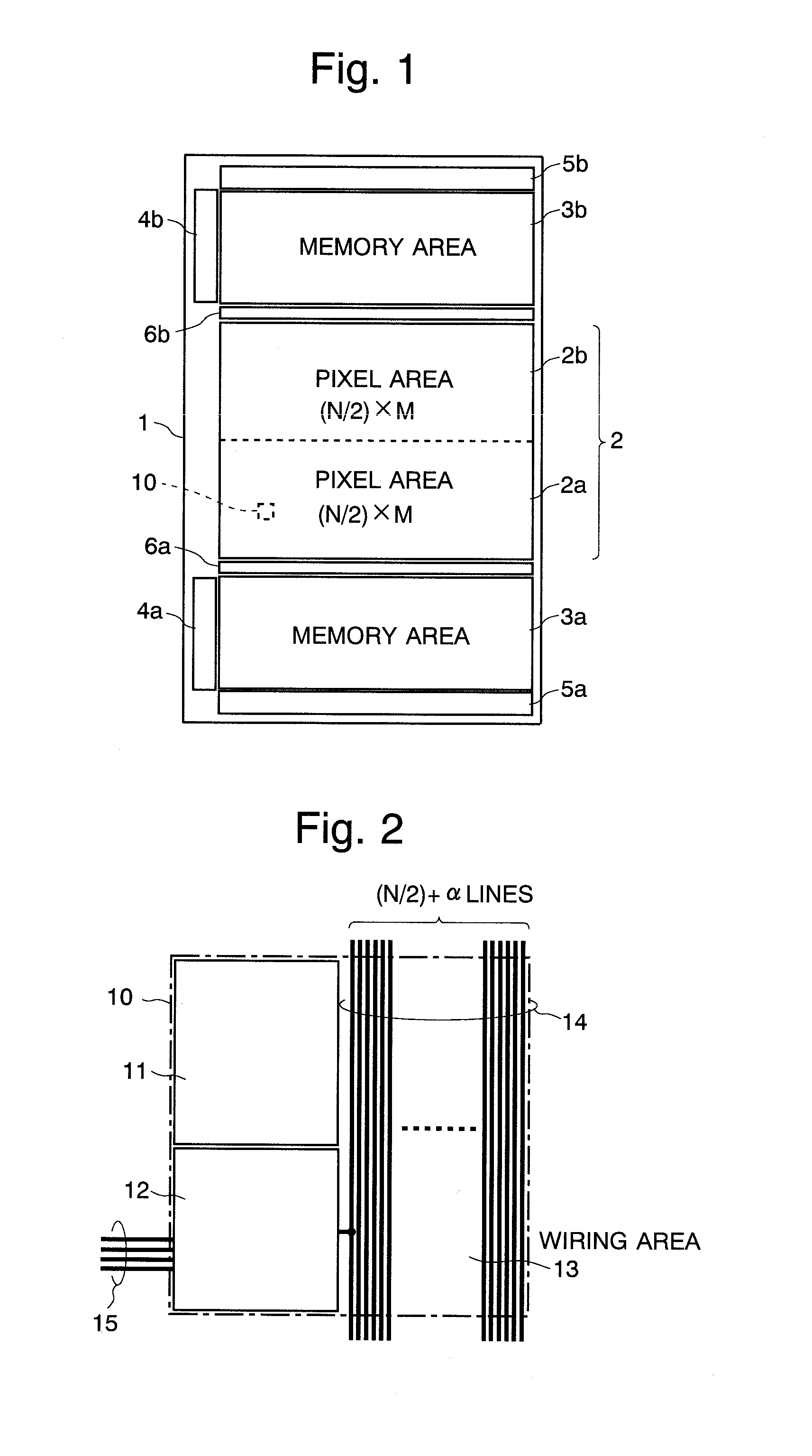
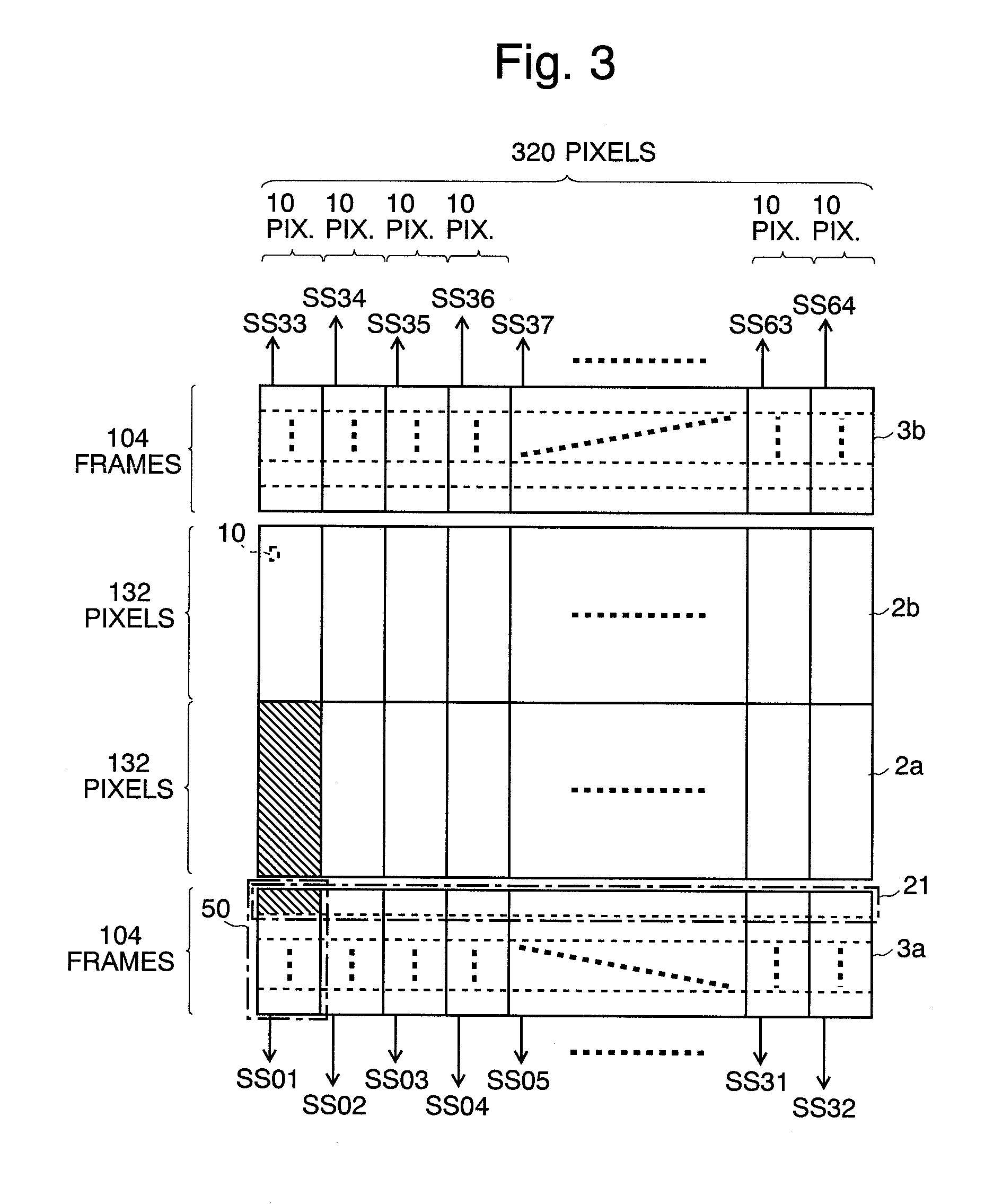
[0065]An overall configuration and structure of the solid-state image sensor according to the present embodiment is initially described. FIG. 1 is a schematic plan view showing the layout on a semiconductor chip of the solid-state image sensor of the present embodiment, FIG. 3 is a plan view showing a schematic configuration of the pixel area and memory area in the solid-state image sensor of the present embodiment, and FIG. 4 is a block diagram of the main portion corresponding to approximately one-half of the semiconductor chip of the solid-state image sensor of the present embodiment.

[0066]As shown in FIG. 1, in the present solid-state image sensor, the pixel area 2 (2a and 2b) for receiving light and producing signals for each pixel and the memory areas 3a and 3b for holding the signals f...


PUM


Abstract

A floating diffusion (331) is created substantially at center of the light-receiving surface of an embedded photodiode (31), with a gate electrode of a transfer transistor (32) surrounding the floating diffusion. The concentration (or depth) of impurities in a p+-type semiconductor region, n-type semiconductor region or p-well region is changed in an inclined form so that a potential gradient being inclined downwards from the circumference to the center is created when an appropriate bias voltage is applied to the pn junction. The photocharges produced by incident light are rapidly moved along the potential gradient toward the center. Even in the case where the photocharge storage time is short, the photocharges can be efficiently collected since the maximum moving distance from the circumference of the photodiode (31) to the floating diffusion (331). Thus, the photocharges produced by the photodiode (31) are efficiently utilized, whereby the detection sensitivity is improved.

Description

CROSS REFERENCE TO RELATED APPLICATIONS[0001]This application is a National Stage of International Application No. PCT / JP2008 / 002428 filed Sep. 4, 2008, claiming priority based on Japanese Patent Application No. 2007-230181, filed Sep. 5, 2007, the contents of all of which are incorporated herein by reference in their entirety.TECHNICAL FIELD[0002]The present invention relates to a solid-state image sensor and a method for producing this sensor. More specifically, it relates to a solid-state image sensor capable of high-speed operations suitable for taking images of high-speed phenomena such as destructions, explosions and combustions, and a method for producing such a sensor.BACKGROUND ART[0003]High-speed imaging devices (high-speed video cameras) for taking consecutive images of high-speed phenomena such as explosions, destructions, combustions, collisions and discharges for only a short period of time have been conventionally developed (for example, refer to Non-Patent Document 1...

Claims


Application Information

Patent Timeline
Patent Type & Authority Patents(United States)
IPC IPC(8): H01L27/148H01L21/00H04N3/14H04N5/335H04N5/374H04N5/3745
CPCH01L27/14603H01L27/14609H01L27/14689H01L27/14612H04N5/374H04N5/37452H04N5/378H04N5/335H01L27/14645H04N25/00H04N25/76H04N25/771H04N25/75
Inventor SUGAWA, SHIGETOSHIKONDO, YASUSHITOMINAGA, HIDEKI
Owner TOHOKU UNIV
Why Eureka
Try Eureka