Implementing mulitple mask lithography timing variation mitigation

a technology of lithography and timing variation, applied in the field of data processing, can solve the problems of difficult printing on very tight pitches, dead hardware, and reduced performance, and achieve the effect of less timing margin, minimizing layout impact of circuits, and improving the timing of paths

Inactive Publication Date: 2013-11-05
GLOBALFOUNDRIES INC
View PDF11 Cites 7 Cited by
  • Summary
  • Abstract
  • Description
  • Claims
  • Application Information

AI Technical Summary

Benefits of technology

[0006]A principal aspect of the present invention is to provide a method, system and computer program product for implementing multiple mask lithography timing variation mitigation. Other important aspects of the present invention are to provide such method, system, and computer program product substantially without negative effects and that overcome many of the disadvantages of prior art arrangements.
[0007]In brief, a method, system and computer program product are provided for implementing multiple mask lithography timing variation mitigation for a multiple mask polysilicon (PC) process. An application specific integrated circuit (ASIC) library includes at least one circuit device for a first mask, and at least one circuit device for a second mask. Critical hold time paths and critical setup time paths are identified in a circuit design. For critical hold time paths, circuit devices in the critical hold time paths are placed on a single mask of either the first mask or the second mask. For critical setup time paths, path delays are reduced by providing a mixture of circuit devices on the first mask and the second mask.
[0010]In accordance with features of the invention, for critical setup time paths where delay needs to be minimized, a mix of both masks is selected. This improves the timing of the paths because the probability that both mask phases vary to make the paths slow is less than the probability that a single mask phase would vary. For example, for each path and all the associated logic, an even distribution or even split between the first mask or the second mask is selected.
[0011]In accordance with features of the invention, the ASIC library minimizes the layout impact of having circuits on two or more different masks.

Problems solved by technology

The emergence of multiple mask lithography for polysilicon is due to the difficulty of printing on very tight pitches.
Otherwise, without adding margin to account for mask variation; dead hardware or reduced performance likely may result.

Method used


Image

  • Implementing mulitple mask lithography timing variation mitigation
  • Implementing mulitple mask lithography timing variation mitigation
  • Implementing mulitple mask lithography timing variation mitigation

Examples


Embodiment Construction

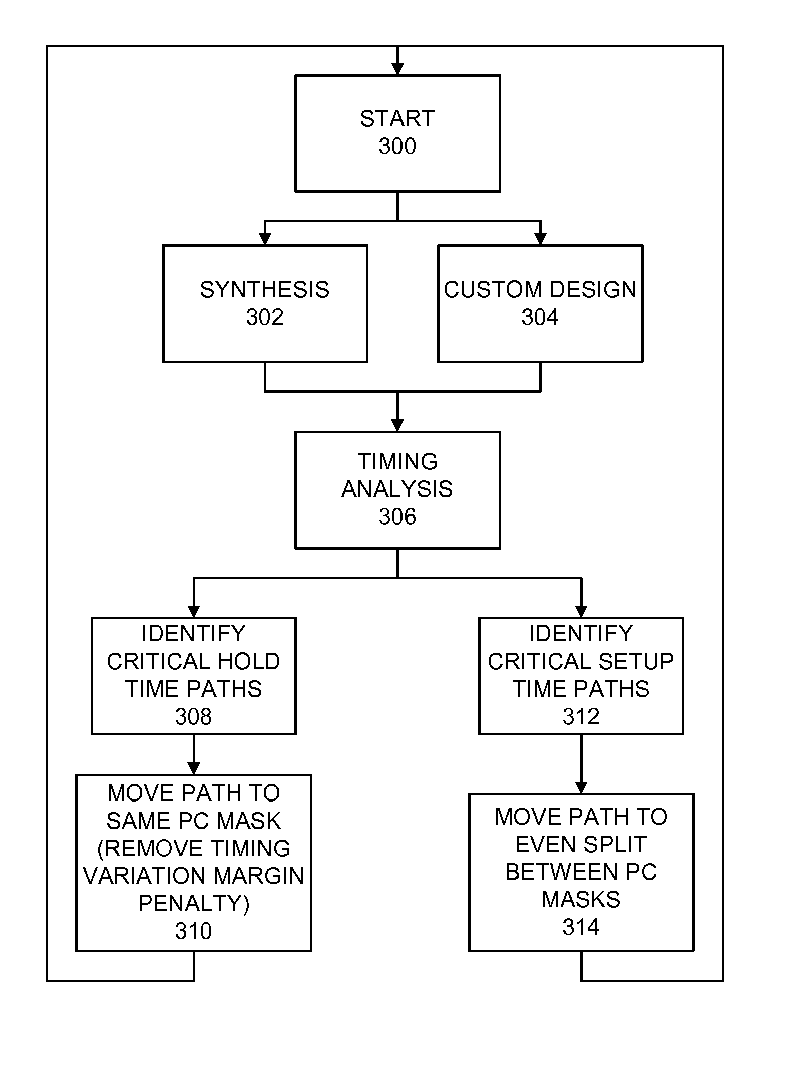
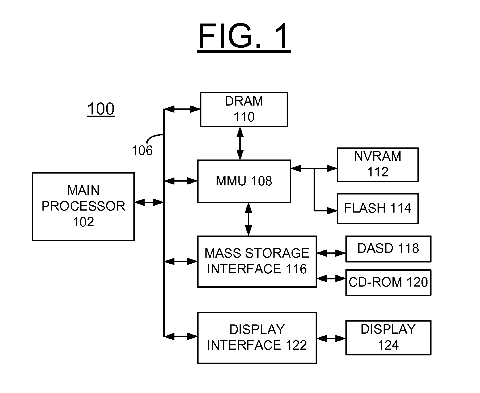
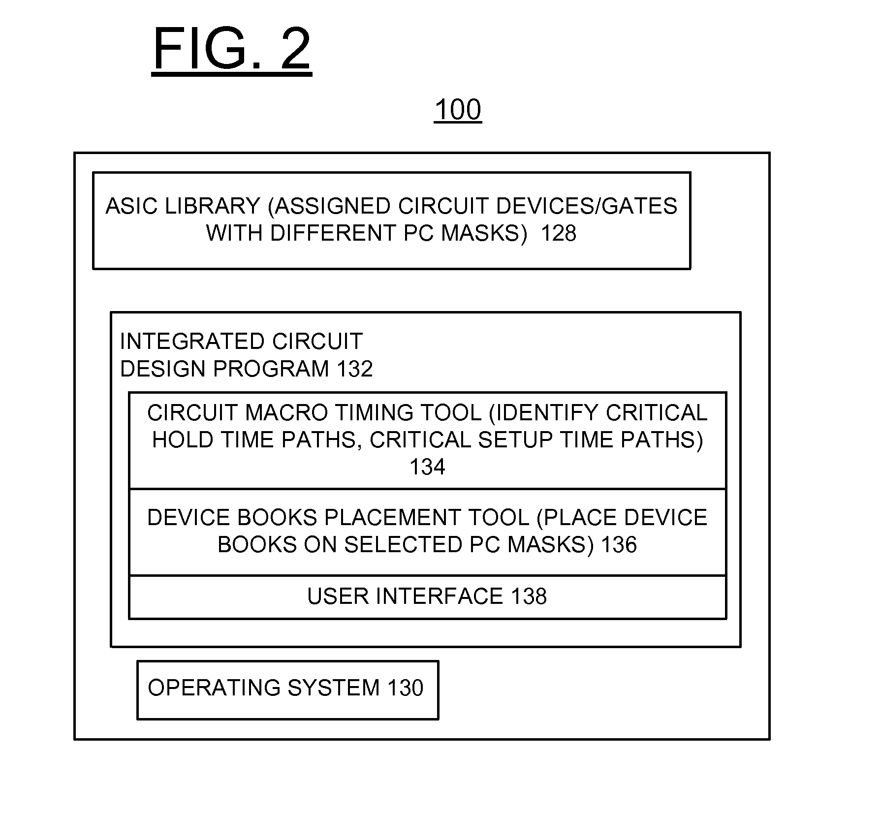
[0018]In the following detailed description of embodiments of the invention, reference is made to the accompanying drawings, which illustrate example embodiments by which the invention may be practiced. It is to be understood that other embodiments may be utilized and structural changes may be made without departing from the scope of the invention.

[0019]The terminology used herein is for the purpose of describing particular embodiments only and is not intended to be limiting of the invention. As used herein, the singular forms “a”, “an” and “the” are intended to include the plural forms as well, unless the context clearly indicates otherwise. It will be further understood that the terms “comprises” and / or “comprising,” when used in this specification, specify the presence of stated features, integers, steps, operations, elements, and / or components, but do not preclude the presence or addition of one or more other features, integers, steps, operations, elements, components, and / or gr...


PUM


Abstract

A method, system and computer program product are provided for implementing multiple mask lithography timing variation mitigation for a multiple mask polysilicon (PC) process. An application specific integrated circuit (ASIC) library includes at least one circuit device for a first mask, and at least one circuit device for a second mask. Critical hold time paths and critical setup time paths are identified in a circuit design. For critical hold time paths, circuit devices in the critical hold time paths are placed on a single mask of either the first mask or the second mask. For critical setup time paths, path delays are reduced by providing a mixture of circuit devices on the first mask and the second mask.

Description

FIELD OF THE INVENTION[0001]The present invention relates generally to the data processing field, and more particularly, relates to a method, system and computer program product for implementing multiple mask lithography timing variation mitigation.DESCRIPTION OF THE RELATED ART[0002]The emergence of multiple mask lithography for polysilicon is due to the difficulty of printing on very tight pitches. In integrated circuit design of modern chips having very small lithography, such as 14 nm, more than one mask, and therefore more than one exposure on a level is required to produce shapes on the level.[0003]The use of multiple mask lithography introduces tracking differences between devices created using a first mask relative to devices created on a second mask. On logic paths where hold times are a concern, very tight tracking is required.[0004]By introducing this multiple mask polysilicon (PC) process, variation between polysilicon (PC) fingers is increased. When two timing paths are...

Claims


Application Information

Patent Timeline
Patent Type & Authority Patents(United States)
IPC IPC(8): G06F17/50
CPCG03F1/70
Inventor BEHRENDS, DERICK G.CHRISTENSEN, TODD A.HEBIG, TRAVIS R.LAUNSBACH, MICHAEL
Owner GLOBALFOUNDRIES INC
Why Eureka
Try Eureka