Controlled penetration subpad

a technology of subpads and sealing pads, which is applied in the direction of flexible wheels, manufacturing equipment/tools, manufacturing tools, etc., can solve the problems of circuitry size, polishing pads that cannot be sanded, and require more stringent requirements

Active Publication Date: 2013-12-10
ROHM & HAAS ELECTRONICS MATERIALS CMP HLDG INC
View PDF16 Cites 12 Cited by
  • Summary
  • Abstract
  • Description
  • Claims
  • Application Information

AI Technical Summary

Benefits of technology

[0011]The invention provides a method of preparing a seamless polishing pad that solves the problem of nonuniform penetration of a hardenable fluid into a porous subpad. The invention also provides a seamless polishing pad comprising a polishing layer having a substantially uniform depth of penetration into a porous subpad.
[0013]A substantially uniform depth of penetration may be achieved by applying a barrier to the subpad before coating the subpad (and barrier) with the hardenable fluid. Preferably, the barrier possesses the following properties: (a) it adheres well to both the subpad and to the polishing layer, (b) it substantially prevents the hardenable fluid from penetrating into the subpad, and (c) it does not substantially alter the compressibility of the subpad.
[0014]According to the method of the present invention, a seamless polishing pad includes a polishing layer having a substantially uniform depth of penetration into a porous subpad can be prepared by (a) providing a porous subpad, (b) applying a barrier to the subpad, and (c) coating the barrier-coated subpad with a hardenable fluid to form a seamless polishing layer. As compared to a polishing pad formed of the same materials according to the same method, but omitting step (b) (i.e., a polishing pad not including a barrier), a polishing pad prepared according to the method of the present invention comprises a polishing layer whose depth of penetration into the porous subpad is more uniform.

Problems solved by technology

The decrease in the size of circuitry and the increase in the number of layers applied are leading to ever more stringent requirements on the smoothness and planarity of the silicon and semiconductor wafers throughout the chip manufacturing process, since uneven surfaces may undermine the patterning process and the general integrity of the resulting circuit.
A disadvantage of such prior art polishing pads is that they often contain seams.
Moreover, the seams can mar the surface of a polished article, and can limit the ability of a pad to polish the article to a high degree of planarity.
This causes air to be displaced from the subpad into the hardenable fluid, which can create voids in the hardened polishing layer.
As discussed earlier in connection with the seam problem, when the properties of the polishing pad are not uniform, it can limit the pad's ability to impart uniform levels of smoothness and planarity to a polished item, whether it be a silicon wafer, an optical component, or another article.

Method used


Image

  • Controlled penetration subpad
  • Controlled penetration subpad
  • Controlled penetration subpad

Examples


example 1

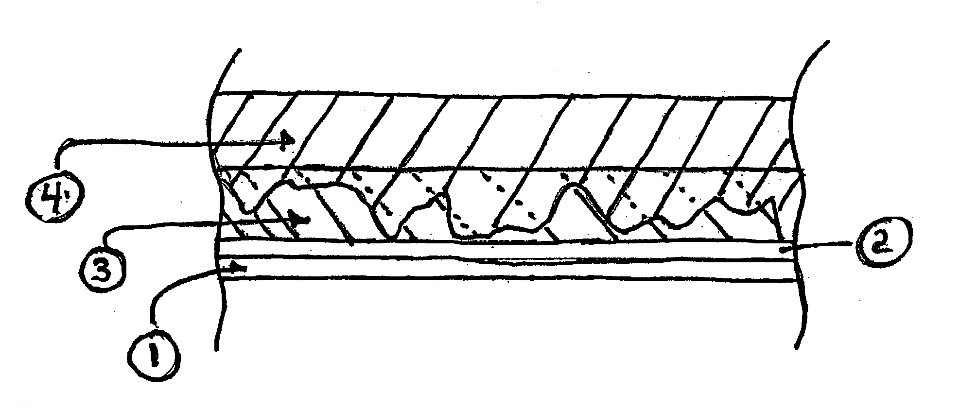
[0072]A polishing belt was produced by casting a polyurethane polishing layer over a commercially available subpad material laminated to an endless stainless steel belt.

[0073]The endless stainless steel belt (substrate 1) was approximately 94 inches long, 13 inches wide, and 0.020 inches thick. The endless stainless steel band in this example was obtained from Belt Technologies Inc. (Agawam, Mass.).

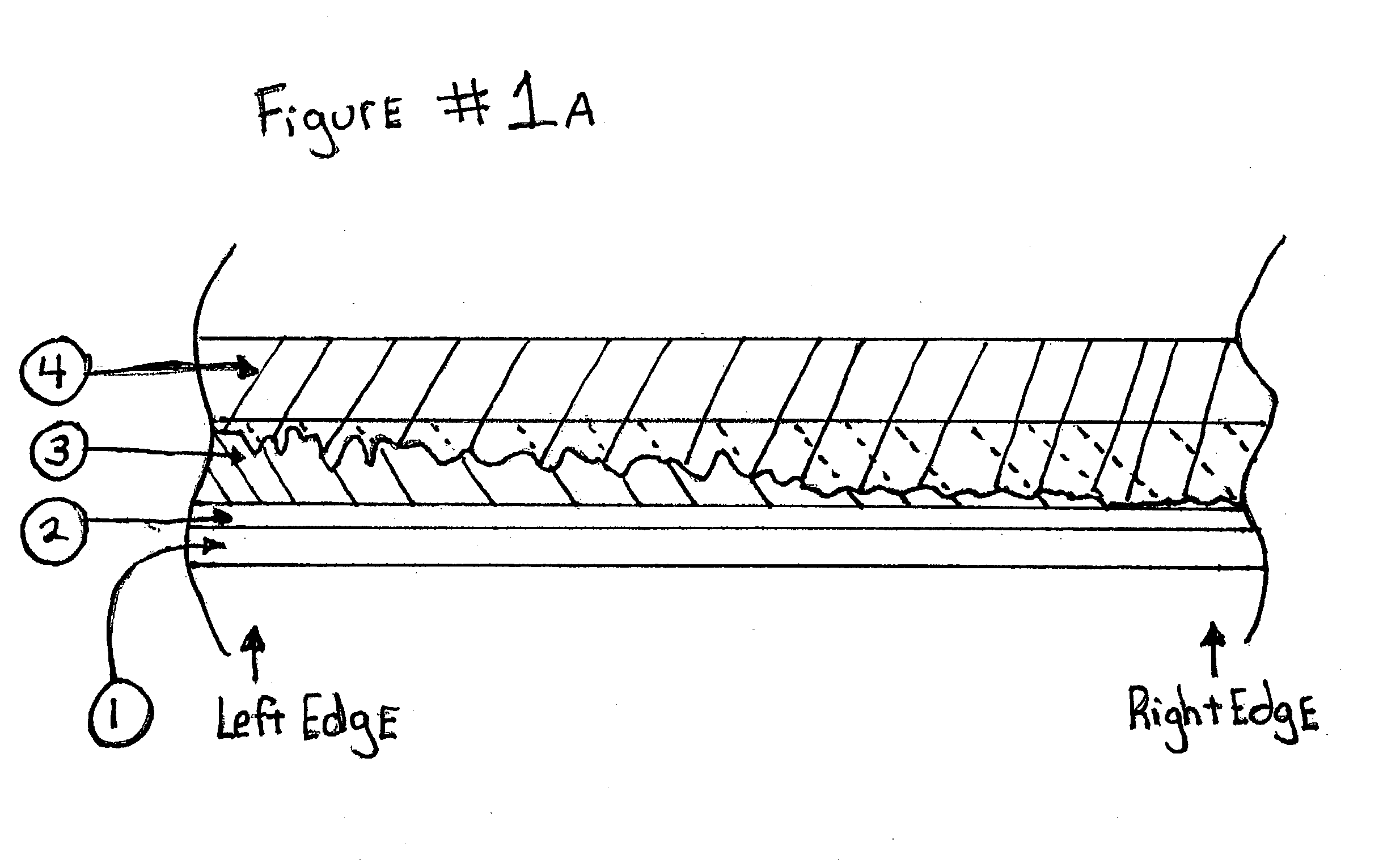
[0074]Subpad 3 in this example was obtained from Thomas West Inc. (Sunnyvale, Calif.). The commercial designation for the subpad is 817. This material is a yellow colored non-woven material, impregnated with a soft elastomeric composition. Despite the impregnation, the subpad material still is porous and compressible. The subpad material was supplied with a rubber-based pressure sensitive adhesive laminated to one side. The subpad was obtained in rectangular pieces approximately 12 inches wide and 31.25 inches long. The thickness of the subpad and adhesive together was approximately 0.028...

example 2

[0091]The method of Example 1 was repeated using a different non-woven material as subpad 3. In this example, a non-woven material called AQUILINE™ and made by TEXON International (Leicester, England), was laminated on one side with the same rubber-based pressure sensitive adhesive 2 as was used in Example 1. The AQUILINE™ material comprises non-woven polyester fibers with much less impregnating material compared to the 817 material from Thomas West Inc. Comparing the two different subpad materials using a microscope or SEM shows that the AQUILINE™ material has a much more open structure and a higher degree of porosity than the 817. The AQUILINE™ subpad was cut into rectangular pieces approximately 12 inches wide and 31.25 inches long. The thickness of the subpad and adhesive together was approximately 0.038 inches, where the subpad layer was approximately 0.032 inches thick, and the adhesive layer was approximately 0.006 inches thick.

[0092]The same methods as described in Example 1...

example 3

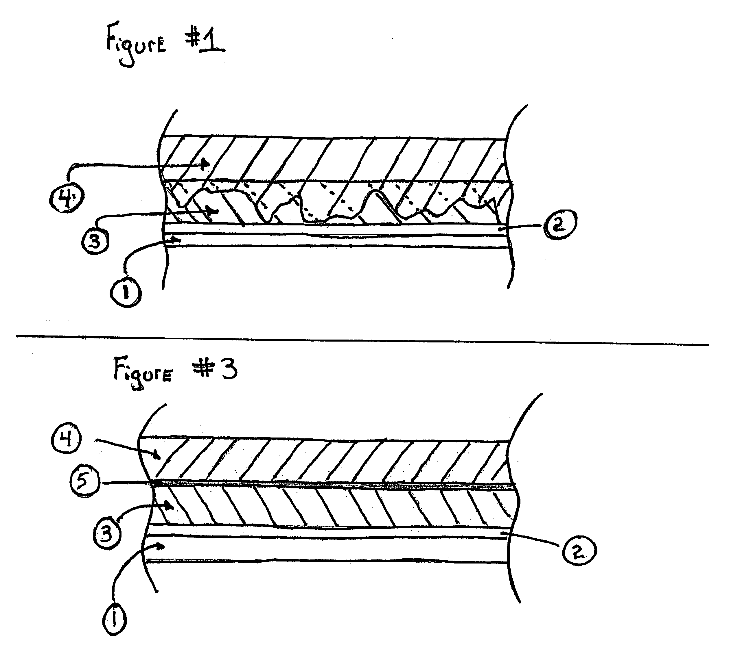
[0097]The method of Example 2 was repeated, except that in this case a barrier 5 was applied to the AQUILINE™ subpad material prior to casting polishing layer 4. A barrier was achieved using a knife-over-roll technique to apply a polyurethane adhesive composition (D2596H Adhesive and D2597 Crosslinker, available from DELA, Inc.) to one side of the non-woven material prior to having the pressure sensitive adhesive laminated to the other side of the non-woven. The barrier material formed a very thin film at the top surface of the non-woven material, adopting the texture and topography of the non-woven and substantially sealing the top surface of the subpad layer. A single belt was used for qualitative peel tests, penetration measurements, hardness measurements, and compressive testing. Other polishing belts were prepared according to the same method, and were used to check lamination integrity on the belt roller apparatus depicted in FIG. 5.

[0098]Qualitative peel testing indicated tha...


PUM

PropertyMeasurementUnit
diameteraaaaaaaaaa
thicknessaaaaaaaaaa
thicknessaaaaaaaaaa

Abstract

Provided is a seamless polishing pad comprising a seamless polishing layer having a substantially uniform depth of penetration into a porous subpad. In one embodiment, the polishing pad comprises a polishing layer produced by applying to the subpad a hardenable fluid. In another embodiment, the subpad is coated with a barrier before coating with the hardenable fluid. In each embodiment, the depth of penetration of the polishing layer and / or barrier is substantially uniform. Also provided is a method of producing a seamless polishing pad comprising a seamless polishing layer having a substantially uniform depth of penetration into a porous subpad.

Description

FIELD OF THE INVENTION[0001]This invention relates to a seamless polishing pad comprising a seamless polishing layer having a substantially uniform depth of penetration into a porous subpad.BACKGROUND OF THE INVENTION[0002]Silicon wafers are produced as precursors from which microelectronic semiconductor components are produced. The wafers are cleaved from cylindrical silicon crystals, parallel to their major surfaces, to produce thin disks, typically 20-30 cm in diameter. The resulting wafers must be polished to give flat and planar surfaces for proper formation of electronic components to form integrated chip semiconductor devices. Typically, a 20-cm diameter wafer will produce 100 or more microprocessor chips.[0003]The designed size of such integrated chips is steadily decreasing, while the number of layers applied, e.g. by various sequences of depositing, patterning, and etching of features onto the silicon surface, is rising. Present semiconductors typically incorporate up to 7...

Claims


Application Information

Patent Timeline
Patent Type & Authority Patents(United States)
IPC IPC(8): B24D11/00B24B21/04B24B37/22B24D13/14
CPCB24B21/04B24B37/22
Inventor LOMBARDO, BRIAN SCOTTCIANCIOLO, JOSEPH
Owner ROHM & HAAS ELECTRONICS MATERIALS CMP HLDG INC
Why Eureka
Try Eureka