High-power semiconductor laser and method for manufacturing the same

a semiconductor laser and high-power technology, applied in the field of laser manufacturing, to achieve the effect of long life, low cost and easy manufacturing

Active Publication Date: 2014-01-28
FOCUSLIGHT TECH
View PDF9 Cites 0 Cited by
  • Summary
  • Abstract
  • Description
  • Claims
  • Application Information

AI Technical Summary

Benefits of technology

[0013]An objective of the invention is to overcome shortcomings associated with conventional single-emitter lasers and the process for making such lasers and to provide a new, high-power semiconductor laser and a method for making the same. A technical problem to be addressed is how to provide lasers that are safe, reliable, low cost and easy to make, have long lifetime and can produce high-power outputs. Such lasers would preferably also have better mechanical reliability and are more suitable for practical use.

Problems solved by technology

A technical problem to be addressed is how to provide lasers that are safe, reliable, low cost and easy to make, have long lifetime and can produce high-power outputs.

Method used


Image

  • High-power semiconductor laser and method for manufacturing the same
  • High-power semiconductor laser and method for manufacturing the same
  • High-power semiconductor laser and method for manufacturing the same

Examples


Embodiment Construction

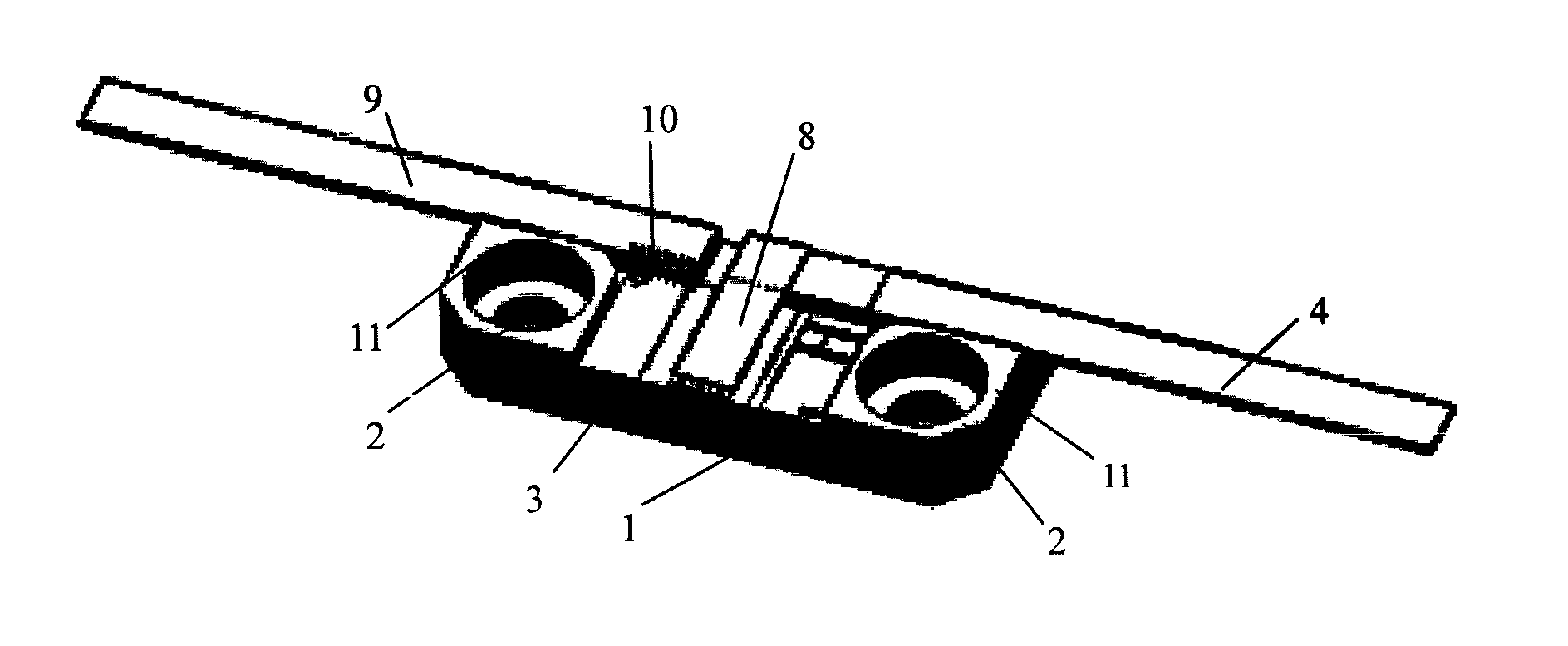
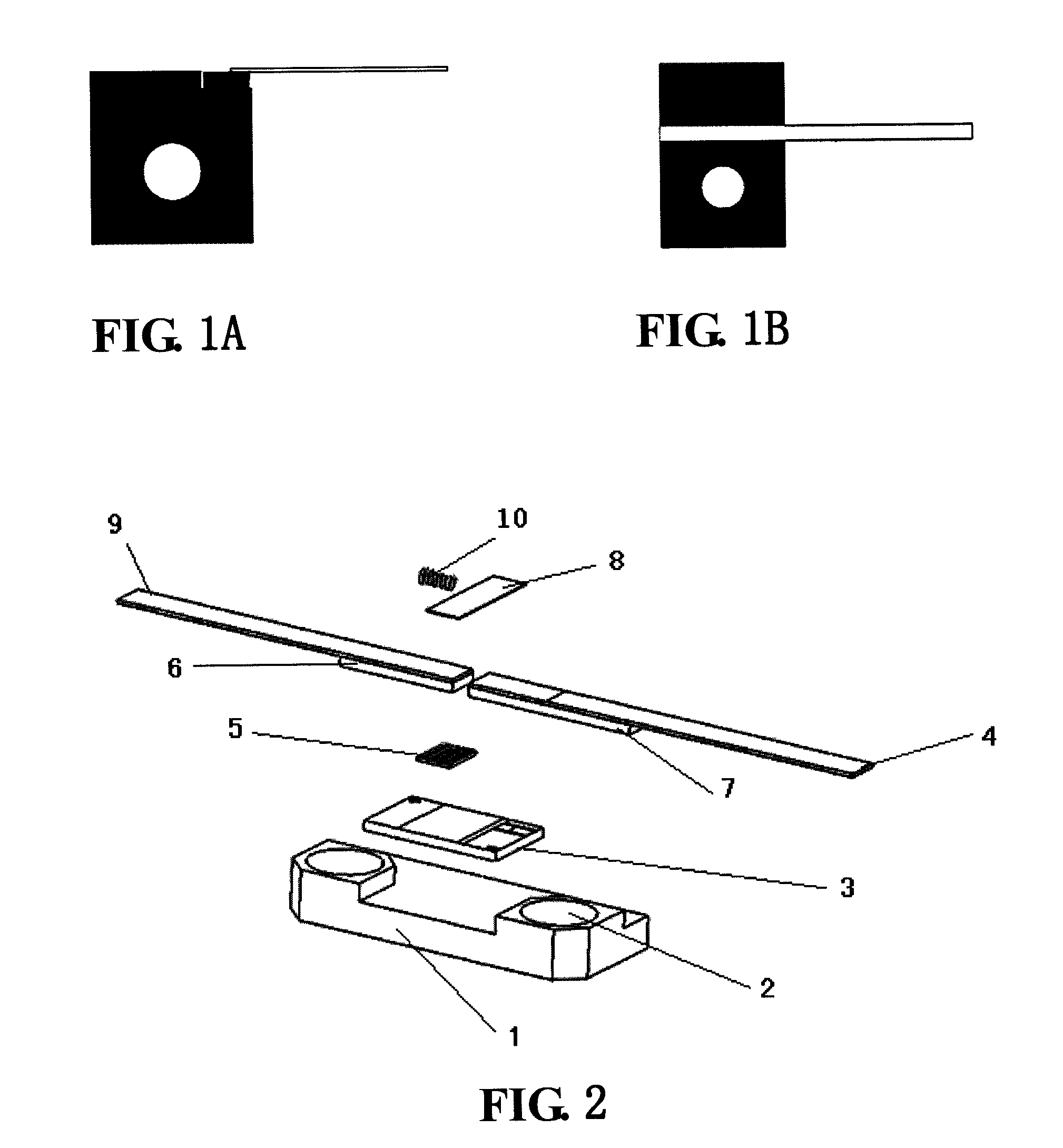
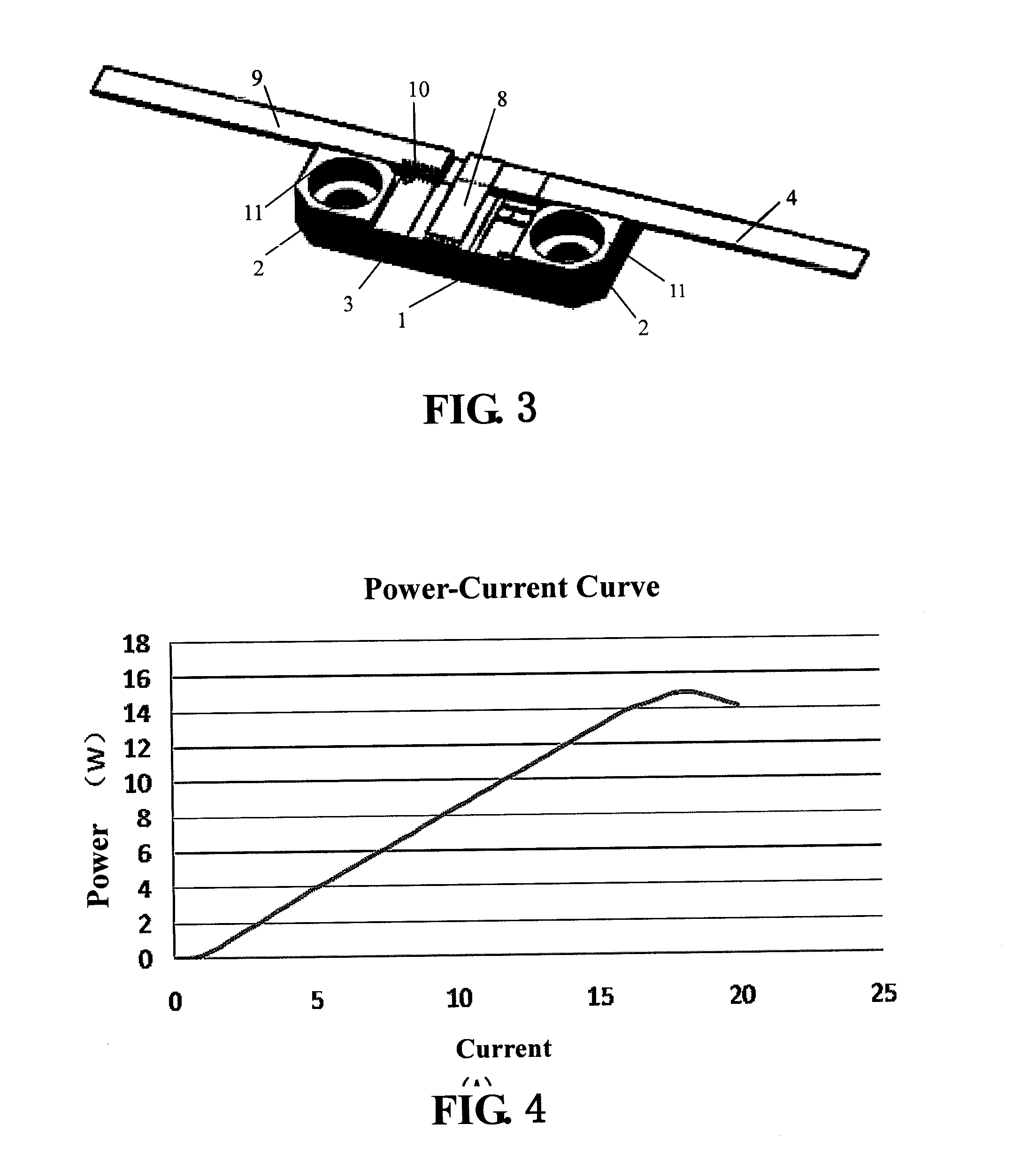
[0066]In accordance with the present invention, a sample 808 nm high-power single-chip semiconductor laser has been built. The wavelength of the light emitted by the semiconductor laser is 808 nm. The structure of this laser is illustrated in FIG. 3. The output power of this laser exceeds 10 W in continuous operation.

[0067]The following are test results of the 808 nm high-power single-chip semiconductor laser:

[0068](1) FIG. 4 shows a P-I curve of the sample 808 nm high-power single emitter semiconductor laser sample. The highest light output of this laser is 15 W.

[0069](2) FIG. 5 show test results of the laser operating to output 6 W power, at which level high reliability of this laser can be ensured. In this test, the working current is 7.38 A, the working potential (voltage) is 1.91V, the threshold current is 0.65 A, the slope efficiency is 0.87 W / A, typical electro-optic conversion efficiency is 41.35%, the maximal electro-optic conversion efficiency is 42.42%, and series resista...


PUM

PropertyMeasurementUnit
thickaaaaaaaaaa
power efficienciesaaaaaaaaaa
thicknessaaaaaaaaaa

Abstract

A high-power semiconductor laser includes a support block, an anode metal plate, a cathode metal plate and a chip. The support block has a step, and the two ends of the support block have bosses, in which there are screw holes. The chip is welded to an insulation plate, which is attached to the support block. The anode metal plate and the cathode metal plate are, respectively, welded with an anode insulation plate and a cathode insulation plate, which are welded on the step of the support block. The cathode of the chip is connected with a metal connecting plate. The metal connecting plate is connected to the anode metal plate and the cathode metal plate. The insulation plate and the anode metal plate are bonded using a gold wire in press-welding.

Description

BACKGROUND OF INVENTION[0001]1. Field of the Invention[0002]The invention relates to laser manufacturing, in particular to a high-power single emitter semiconductor laser and methods for manufacturing the same.[0003]2. Background[0004]Semiconductor laser is also called laser diode (LD). In 1980s, based on new developments in physics, such as new structures based on quantum well (QW) and strained-layer quantum well (SL-QW), refractive index modulation Bragg transmitters were developed and improved. At the same time, new crystal growth techniques, such as MBE, MOCVD and CBE, were also developed. All of these developments allowed new epitaxial techniques to precisely control crystal growth, enabling one to achieve thickness precision down to the molecular layer level, and to produce high-quality QW and SL-QW materials. Therefore, LDs made from these materials had markedly reduced the current threshold, significantly enhanced conversion efficiency, greatly improved power output, and mar...

Claims


Application Information

Patent Timeline
Patent Type & Authority Patents(United States)
IPC IPC(8): H01S5/022H01S5/024
CPCH01L2924/01013H01L2924/0105H01L2924/01078H01S5/02272H01L2924/01079H01S5/02476H01L2924/01004H01L2224/85203H01L2224/45144H01L2924/00014H01S5/0237H01L2224/48
Inventor LIU, XINGSHENG
Owner FOCUSLIGHT TECH
Why Eureka
Try Eureka