Carbon nanotube device and process for producing the same
a carbon nanotube and process technology, applied in the field of carbon nanotube devices and process for producing the same, can solve the problems of difficult search for an appropriate support condition of a catalyst, large mixing of catalysts, aggregation and coarsening under, etc., and achieve the effect of reducing the space of the layer, reducing the mixing of impurities in carbon nanotubes, and simplifying the process
- Summary
- Abstract
- Description
- Claims
- Application Information
AI Technical Summary
Benefits of technology
Problems solved by technology
Method used
Image
Examples
first embodiment
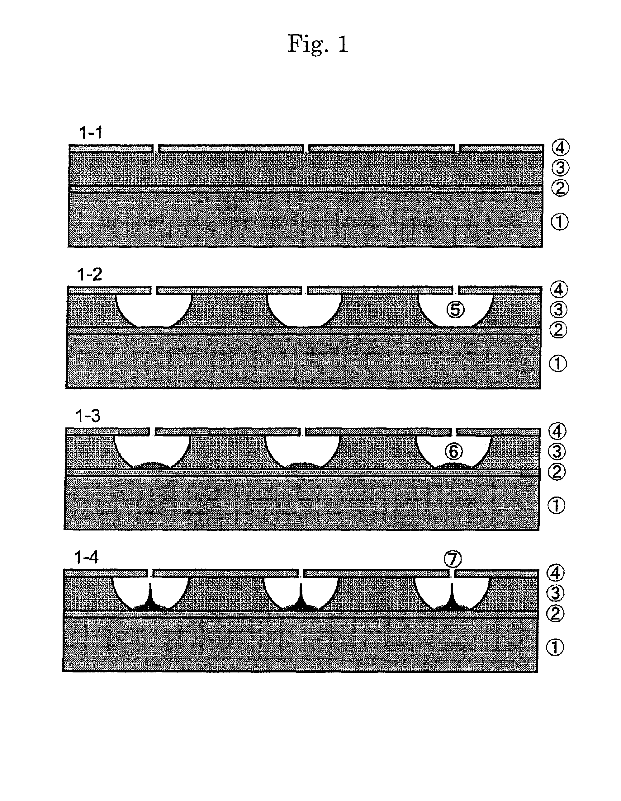
[0047]FIG. 1 is a cross-sectional view illustrating the structure of a carbon nanotube device in production steps according to an embodiment of the invention.
[0048]The carbon nanotube device of the embodiment has a conductive film (2) formed on a substrate (1), an insulating film (3) with holes (5) formed on the conductive film, and a coating film (4) formed on the insulating film. Catalyst substances (6) are used in the production steps, and spiny carbon nanotube aggregates (7) extend from the conductive film (2) exposed with respect to the holes (5) toward the tiny openings of the coating film (4).
[0049]Note that the coating film (4) may be omitted. The substrate (1) and the conductive film (2) may be considered as one “substrate” as a whole. In this case, the conductive film (2) which is a surface of the “substrate” is exposed by the holes (5). In a case where it is considered that the substrate (1) and the conductive film (2) are separate demonstratively, the holes (5) also erod...
second embodiment
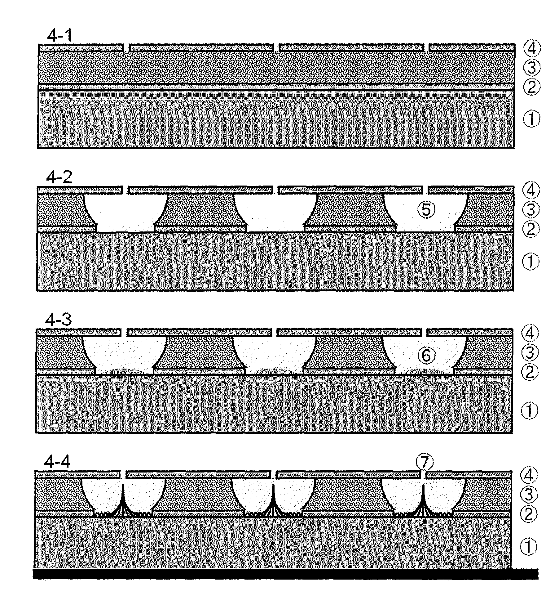
[0100]FIG. 4 is an explanatory diagram illustrating a modified example of the foregoing embodiment. An explanation will be given with reference to this figure. A carbon nanotube device of the embodiment has the conductive film (2) formed on the substrate (1), the insulating film (3) formed thereon, and the coating film (4) formed thereon. The holes (5) in the embodiment penetrate both insulating film (3) and conductive film (2), and the substrate (1) is exposed with respect to the holes (5).
[0101]The catalyst substances (6) are used in the production steps, and the spiny single-walled carbon nanotube aggregates (7) extend from the conductive film (2) exposed with respect to the holes (5) toward the tiny openings of the coating film (4).
[0102]As typical materials, a silicon substrate with an oxide film is used for the substrate (1), an Mo film (Mo, W, or the like) is used for the conductive film (2), a silicon dioxide film is used for the insulating film (3), a conductive chrome film...
third embodiment
[0115]FIG. 5 is an explanatory diagram illustrating a modified example of the foregoing embodiments. A carbon nanotube device of the embodiment has the conductive film (2) formed on the substrate (1), the insulating film (3) with the holes (5) formed thereon, and the coating film (4) formed thereon. In the production steps, the catalyst substances (6) are used, and the spiny single-walled carbon nanotube aggregates (7) extend from the conductive film (2) exposed with respect to the holes (5) toward the openings of the coating film (4).
[0116]As typical materials, a silicon substrate with an oxide film is used for the substrate (1), an Mo film (Mo, W, or the like) is used for the conductive film (2), a silicon dioxide film is used for the insulating film (3), a conductive chrome film is used for the coating film (4), and silicon dioxide and Co, Fe, Ni, Mo, or the like is used for the catalyst substance (6).
[0117]Although major part of the invention is the same as that of the embodimen...
PUM
| Property | Measurement | Unit |
|---|---|---|
| temperature | aaaaa | aaaaa |
| temperature | aaaaa | aaaaa |
| thickness | aaaaa | aaaaa |
Abstract
Description
Claims
Application Information


