

Power overlay structure with leadframe connections
a power overlay and leadframe technology, applied in semiconductor devices, semiconductor/solid-state device details, electrical apparatus, etc., can solve problems such as failures of solder joints and easy early failure of connections, and achieve high reliability
- Summary
- Abstract
- Description
- Claims
- Application Information
AI Technical Summary
Benefits of technology
Problems solved by technology
Method used
Image

Examples
Embodiment Construction
[0016]Embodiments of the present invention provide for a semiconductor device package having leadframe connections incorporated therein, as well as a method of forming such a semiconductor device package. The semiconductor device package is manufactured such that the leadframe connections form a highly reliable interconnection structure, usable in a variety of high stress environments, for attaching the semiconductor device package to an external circuit.
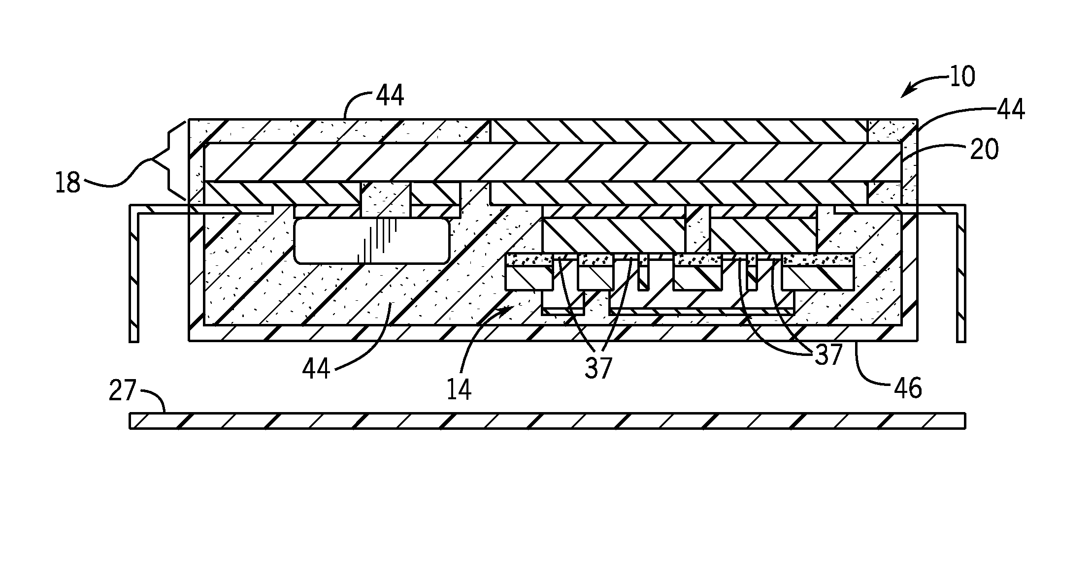
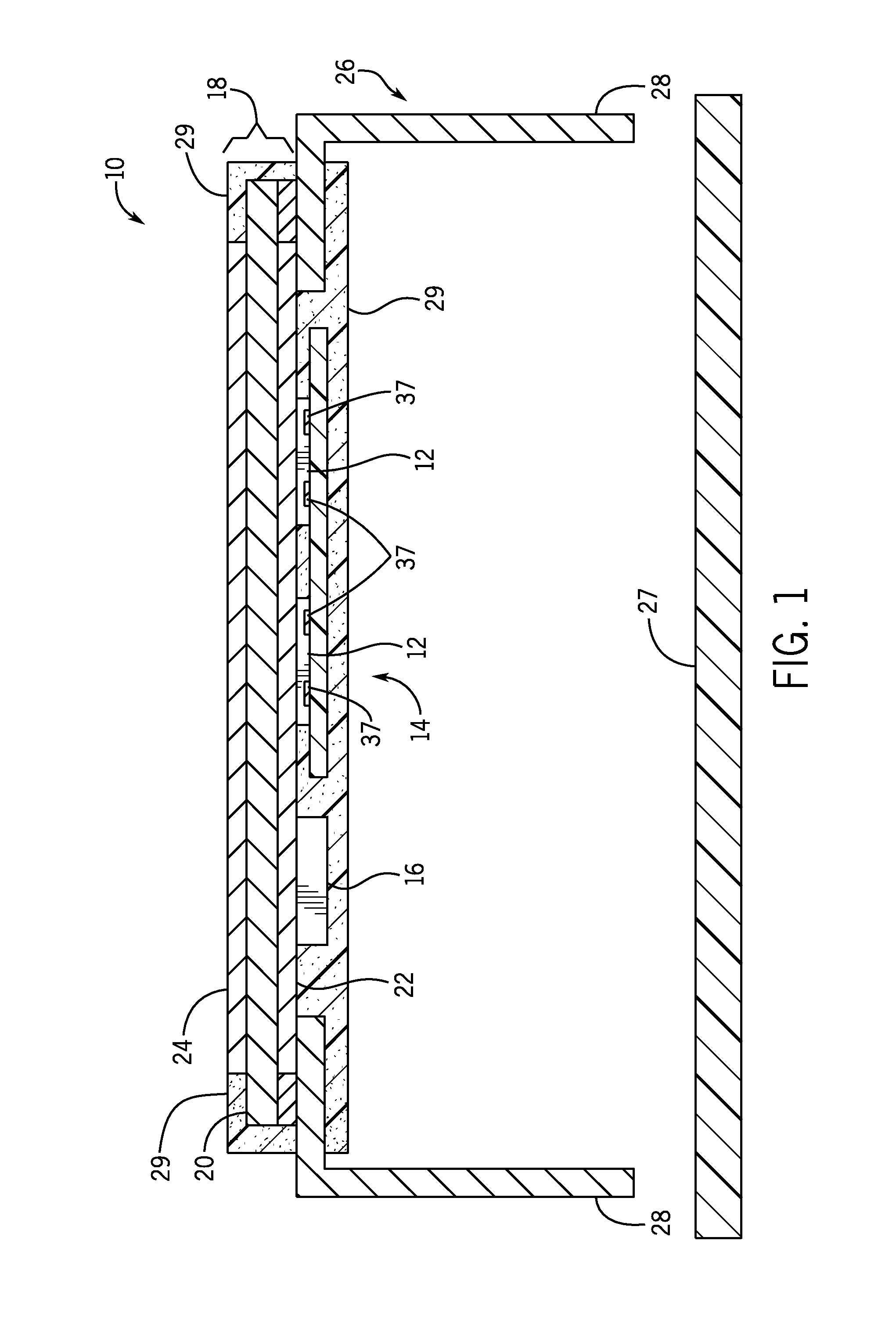
[0017]Referring to FIG. 1, a power overlay (POL) packaging and interconnect structure 10 is shown according to an embodiment of the invention. The POL structure 10 includes one or more semiconductor device(s) 12 therein that, according to various embodiments, may be in the form of a die, diode, or other power electronic device. As shown in FIG. 1, two semiconductor device(s) 12 are provided in POL structure 10, however, it is recognized that a greater or lesser number of semiconductor devices 12 could be included in POL structure 10...
PUM
 Abstract
Description
Claims
Application Information