Optical fiber, method of preparation thereof and device

a technology of optical fiber and optical fiber, applied in the field of optical fiber, can solve the problems of large production cost, inability to adapt to the needs of different applications, and inability to achieve the effect of facilitating a series production of arbitrary patterns

Active Publication Date: 2014-03-11
STICHTING VU
View PDF6 Cites 0 Cited by
  • Summary
  • Abstract
  • Description
  • Claims
  • Application Information

AI Technical Summary

Benefits of technology

[0005]As a first exemplary procedure in the way to solve this problem, it is possible to provide an exemplary embodiment of a process and system which can facilitate a series production of arbitrary patterns on a photoresist layer deposited on the cleaved end of an optical fiber or other surfaces. Such exemplary system and method can utilize an align-and-shine photolithography procedure according to the invention. The align-and-shine photolithography technique is based on the idea to combine standard optical lithography with the opto-mechanical methods developed for optical fiber fusion splicing or similar automatic alignment processes.
[0006]The invention provides an optical fiber, wherein a distal end of the optical fiber is provided with an optical mask adapted for projecting a predetermined pattern on a target surface by radiation transmitted from the distal end of the optical fiber. Such a masked optical fiber having a specific pattern can be used to selectively irradiate a photoresist material deposited on a target surface, in particular the distal end of a target optical fiber. The optical fiber according to the invention enables to construct patterns or structures in a fast and convenient way. In particular, functional patterns or structures can be applied to surface of a target fiber, for instance optically functional elements or patterns, adding functionalities such as a collimator, diffractor, diffuser, filter or other patterns capable of influencing radiation such as visible light, that may be transmitted through the target fiber. The optical fiber according to the invention also allows for applying functional patterns or structures to other surfaces, for instance optical elements such as mirrors and filter surfaces. Preferably, the predetermined pattern has a resolution smaller than 100 nm, allowing to apply fine patterns to relatively small surfaces, which are necessary to obtain certain optical effects. Photoresist materials may be either positive or negative photoresist materials. Positive photoresist materials are characterised in that the portion of the photoresist exposed to irradiation (typically UV-light) becomes soluble to a solvent, and the exposed portion may be washed off afterwards. The portion of the photoresist that is unexposed to the irradiation remains insoluble to the solvent and remains on the target surface. A negative resist is a type of photoresist in which the portion of the photoresist that is exposed to irradiation becomes insoluble to the solvent (for instance by curing or crosslinking a polymer), whereas the unexposed portion may be washed off. Some well known photoresist materials are PMMA (polymethylmethacrylate), PMGI (PolyMethylGlutarimide), DNQ / Novolac (a phenol formaldehyde resin), and SU-8 (an epoxy-based negative photoresist).
[0010]In a further preferred embodiment, the predetermined pattern is adapted for projecting at least one layer of a three-dimensional structure or for projecting a protective layer in the construction of a three-dimensional layer. Such a predetermined pattern is adapted for applying a selective protective layer at a target surface in the layerwise construction of a three-dimensional structure. By layerwise construction, the optical fiber according to the invention enables the easy and rapid construction of three-dimensional structures from various materials. The protective layer made of a photoresist material enables the selective deposition of structural materials and / or selective protection of the underlying material from abrasive techniques such as plasma etching or reactive ion etching. The method according to the invention is particularly useful for rapidly applying selectively protective layers on the target fiber, after which the actual structural material layers such as silicon may be applied by conventional techniques for instance vapor-deposition techniques. The protective layer may be removed, for instance by a suitable chemical agent. For instance certain polymer materials such as PMMA may be removed by organic solvents such as acetone.
[0011]It is preferred if the optical mask is adapted for projecting a predetermined pattern on a target surface, the target surface being a distal end of a target optical fiber. Such a masked optical fiber enables the easy application of the predetermined pattern using a photoresist material on the distal end of the target optical fiber, for instance by selective radiation through the optical mask onto a positive or negative photoresist material, and subsequent removal of soluble material, leaving the predetermined pattern on the target surface. Distal end of optical fibers typically have a diameter in the range from a few mm to as small as the pm range, thus the pattern provided by the optical mask may be of similar proportions.
[0016]providing a masked optical fiber, wherein a distal end of the masked optical fiber is provided with an optical mask having a predetermined pattern, application of a layer of photoresist material to at least part of the target surface, positioning the distal end of the optical fiber with respect to the part of the target surface provided with photoresist material, the application of suitable irradiation through the masked optical fiber to obtain the predetermined pattern in at least part of the photoresist material on the target surface, and the removal of redundant photoresist material. This method allows for a rapid, easy replication of the predetermined pattern on target surfaces. Preferably, the target surface is a distal end of a target optical fiber. The preferred patterns have an optical functionality.
[0020]In a preferred embodiment, the method comprises the steps of growing and patterning alternate layers of sacrificial materials and structural materials on the target fiber. In this preferred embodiment, sacrificial (e.g., phosphosilicate glass, silicon dioxide, et cetera) and structural (e.g., silicon, silicon dioxide, silicon nitride) layers are alternatively deposited on top of the target fiber. Between one deposition and the following one, if necessary, it is possible to remove at least one part of the sacrificial or structural layer according, for example, to the following procedure: providing a first masked optical fiber, wherein a distal end of the optical fiber provided with a first optical mask having a first predetermined pattern, positioning the distal end of target optical fiber with respect to the part of the target surface, wherein the target surface is coated at least in part with at least a sacrifial or structural material layer covered with photoresist material, the application of suitable irradiation through the masked optical fiber to induce the predetermined pattern in the photoresist material on the target surface, the removal of redundant photoresist material to yield a first selectively protective photoresist layer; subsequently followed by the selective removal of the sacrificial or the structural material that is not protected by the patterned photoresist layer by means of, for example, plasma etching or reactive ion etching, and removal of the protective layer from the target surface to enable further layer construction steps. Complex three dimensional structures can be obtained by such a method, in a way similar to what is commonly already done in MicroElectroMechanical Systems technology. The method allows for rapid serial production of patterns or three dimensional elements on a surface, which offers excellent control of the thickness of structural and sacrificial layers, at a relatively high pattern resolution.

Problems solved by technology

Unfortunately, the advantages offered by those instruments may be hampered by the large costs of production, which can be due to the fact that, at present, there are no known versatile fabrication procedures for batch manufacturing of arbitrary micromachined parts on the facet of optical fibers.
The application of this process for the fabrication of patterns on top of optical fibers requires a precise alignment of the lithography mask to the centre of the fiber, which is a too cumbersome operation if standard photolithography mask aligners are to be used.

Method used


Image

  • Optical fiber, method of preparation thereof and device
  • Optical fiber, method of preparation thereof and device
  • Optical fiber, method of preparation thereof and device

Examples


Embodiment Construction

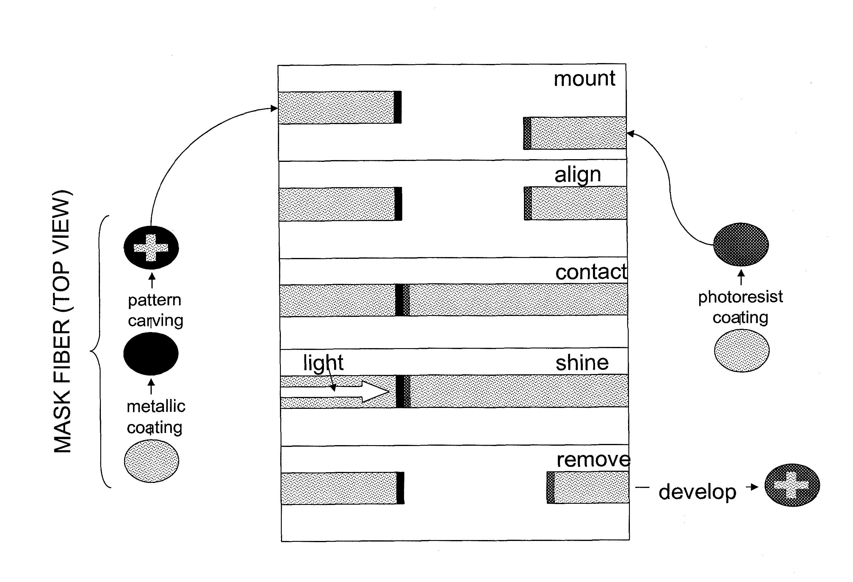
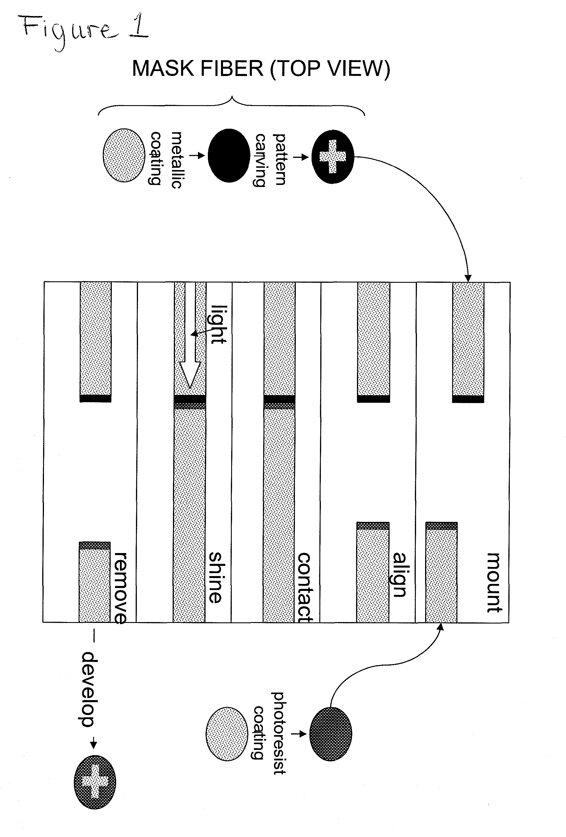
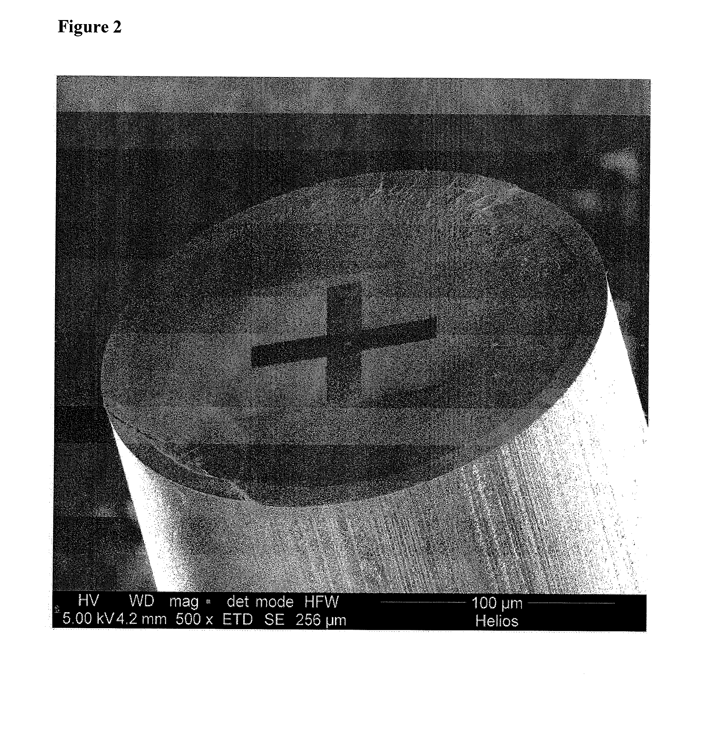
[0030]FIG. 1 shows a flow diagram of an exemplary embodiment of the align-and-shine photolithography procedure according to the present invention. For example, as shown on a left side of FIG. 1, a masked fiber could be an ultraviolet multimode fiber which can be first coated with a metallic layer, which metallic layer may then selectively be removed only along the pattern that must be reproduced on the target fiber. The target fiber (on a right side of FIG. 1) can be coated with photoresist. Thus, the lithography shadow mask can be fabricated directly on the cleaved end of the ultraviolet multimode fiber (e.g., the mask fiber), which may be aligned with another fiber coated with photoresist (e.g., the target fiber). Such two fibers may be mounted on an optical splicing machine, where they can be aligned and brought to contact. The pattern may be transferred from the mask fiber to the target fiber by shining, e.g., an ultraviolet light from the opposite side of the mask fiber. The ta...


PUM

PropertyMeasurementUnit
wavelengthaaaaaaaaaa
diameteraaaaaaaaaa
diameteraaaaaaaaaa

Abstract

The invention provides an optical fiber, a method for the preparation thereof, and a device. An optical fiber, wherein a distal end of the optical fiber is provided with an optical mask adapted for projecting a predetermined pattern on a target surface by radiation transmitted from the distal end of the optical fiber, allows for the rapid application of patterns and three-dimensional structures on target surfaces, in particular on the ends of optical fibers.

Description

CROSS-REFERENCE TO RELATED APPLICATIONS[0001]This application is the National Stage of International Application No. PCT / NL2009 / 050701, filed Nov. 19, 2009, which claims the benefit of U.S. Provisional Application No. 61 / 117,503, filed Nov. 24, 2008.FIELD OF THE INVENTION[0002]The invention provides an optical fiber, a method for the preparation thereof, and a device.BACKGROUND OF THE INVENTION[0003]The shaping of the cleaved end of an optical fiber has been previously described, e.g., in the form of micromachined focusing elements (M. Sasaki et al., Direct photolithography on optical fiber end, Jpn. J. Appl. Phys. 41, 4350-4355 (2002); P. N. Minh et al., Batch fabrication of microlens at the end of optical fiber using self-photolithography end etching technique, Opt. Rev. 10, 150-154 (2003); F. Schiappelli et al., Efficient fiber-to-waveguide coupling by a lens on the end of the optical fiber fabricated by focused ion beam milling, Microelectronic Eng. 73-74, 397-404 (2004); R. S. ...

Claims


Application Information

Patent Timeline
Patent Type & Authority Patents(United States)
IPC IPC(8): G02B6/42G03F7/20G03F1/00
CPCG02B6/262G03F7/7035G03F7/0005G02B6/02061
Inventor IANNUZZI, DAVIDEPETRU{HACEK OVER (S)}IS, AUDRIUSRECTOR, JAN HENDRIK
Owner STICHTING VU
Why Eureka
Try Eureka