Extended wavelength digital alloy NBN detector

a digital alloy and detector technology, applied in the field of photodetectors, can solve the problems of high cost, high energy consumption, and high cost, and achieve the effects of short cutoff wavelength, reasonable quantum efficiency, and different lattice constan

Inactive Publication Date: 2014-03-18
LOCKHEED MARTIN CORP
View PDF14 Cites 12 Cited by
  • Summary
  • Abstract
  • Description
  • Claims
  • Application Information

AI Technical Summary

Benefits of technology

[0016]According to aspects of the present invention, the material forming the plurality of strain-compensation layers exhibit a substantially different lattice constant than that of both the substrate and the remaining absorber material. These thin layers have an aggregate strain substantially equal to the aggregate strain of the photo-absorbing layers but of opposite sign, thereby compensating for the strain of the absorber material. This allows for the growth of sufficiently thick aggregate photo-absorbing layers which do not contain dislocations in the lattice structure of the semiconductor alloy comprising the photo-absorbing layers. The resultant strain-compensated structure of the photodetector allows for the use of an absorber alloy exhibiting a different lattice constant than the lattice constant of the substrate while exceeding the critical thickness at which the lattice structure normally dislocates. The relationship between the critical thickness with respect to increasing strain and eventual dislocations between lattice-mismatched materials is described, for example, in J. W. Matthews and A. E. Blakeslee, J. Cryst. Growth 27, 118 (1974), the entire contents of which are incorporated herein by reference.
[0017]More specifically, according to aspects of the present invention, the strain-compensation layers may be grown alternately with the photo-absorber alloy using epitaxial techniques. The strain-compensation layers are grown sufficiently thin such that they are substantially transparent in quantum-mechanical effect and do not significantly affect the spectral properties of the overall photo-absorbing region. This allows for growth of a photo-absorbing region sufficiently thick to have reasonable quantum efficiency and without exhibiting the dislocation defects that normally would be caused by excessive strain within the absorber alloy. This allows the photodetector to operate beyond the cutoff wavelength of a photodetector with an absorber layer comprising a traditional alloy lattice-matched to the substrate. Similarly one can achieve shorter cutoff wavelengths than the lattice matched alloy, if desirable.
[0023]In a further embodiment of the present invention, a strain-balanced two-color photodetector is provided, which can detect infrared light within two radiation bands each having a different cutoff wavelength. According to the features of this embodiment, at least one of a first layer (photo-absorbing layer) and a second layer (contact layer) located above the barrier layer is grown substantially lattice-mismatched to the substrate and / or the barrier layer. Either or both of the first and second layers may comprise a plurality of strain-compensating layers interspersed between a plurality of photo-absorbing layers so as to substantially compensate for a mechanical strain of the photo-absorbing layers caused by the lattice-mismatched condition. The first layer can exhibit a first cutoff wavelength and the second layer can exhibit a second cutoff wavelength, wherein the first cutoff wavelength can be shorter than the second cutoff wavelength.
[0029]In a further embodiment of the present invention, a photodetector is provided where the minority carrier bandedge of at least one of the first and second layers can be graded vertically by varying the alloy composition in a direction toward the barrier layer. A plurality of varying strain-compensating layers can be interspersed within a graded layer such that the lattice structure is substantially prevented from dislocating. In certain embodiments of the present invention, the interval between the strain-compensating layers in the graded layer can be gradually varied in the direction toward the barrier layer in order to balance the varying strain within the graded layer. In other embodiments of the present invention, the thickness of the strain-compensating layers in a graded layer can be gradually varied in the direction toward the barrier layer in order to balance the varying strain within the graded layer. Alternatively, both of the thickness and periodicity of the strain-compensation layers may be varied in order to balance the varying strain within a graded layer.

Problems solved by technology

However, these thermal detectors require cooling to cryogenic temperatures of around 77 K, which is complex, energy and volume consuming, and costly.
If the lattice constant of the absorber alloy does not match the lattice constant of the substrate material, the strain on the composition of the absorber due to the mismatch between the absorber and substrate lattice structures will increase as the absorber is grown, and will ultimately result in dislocations in the layers of the absorber lattice once the absorber exceeds a critical thickness.
However, this cutoff wavelength falls well short of the upper end of the 3 to 5 μm range for MWIR detection applications operating within the atmospheric window of the infrared band.
However, in a lattice-mismatched condition defects occur in the crystal structure of the absorber when the absorber lattice dislocates to relieve the excess strain resulting from the lattice mismatch between the absorber and the substrate.
These crystalline defects directly effect the operating characteristics of the photodetector device, degrading the quality, e.g. the radiative efficiency and thermal noise, of the semiconductor.
However, this approach can result in poor absorber material quality or a complicated growth processes.
However, the high strain resulting from this approach limits the absorber thickness and material quality.
However, the complicated growth and the band edges of the superlattice system relative to the barrier have made it difficult to achieve MWIR barrier detectors with superlattice absorbers.

Method used


Image

  • Extended wavelength digital alloy NBN detector
  • Extended wavelength digital alloy NBN detector
  • Extended wavelength digital alloy NBN detector

Examples


Embodiment Construction

[0057]The following detailed description of the invention refers to the accompanying drawings. The same reference numbers in different drawings identify the same or similar elements. Also, the following detailed description does not limit the invention. Instead, the scope of the invention is defined by the appended claims and equivalents thereof.

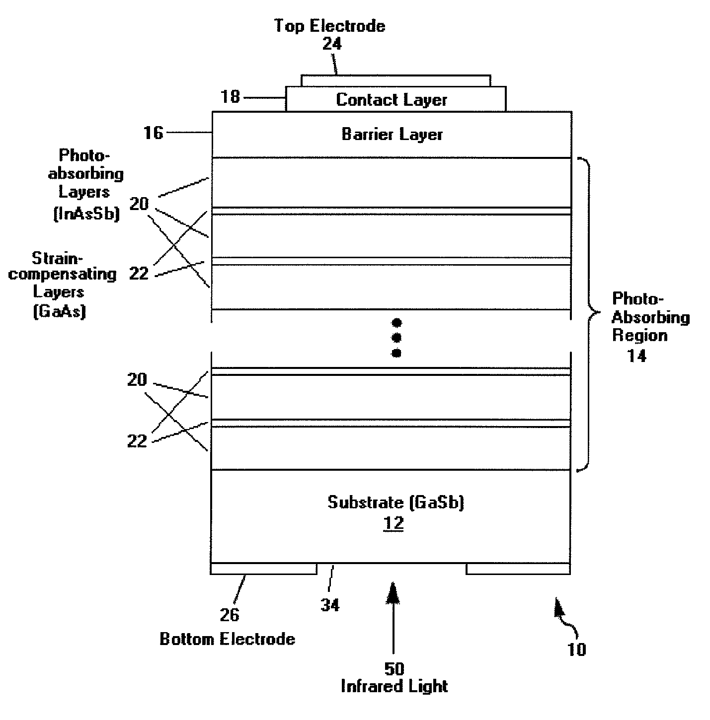
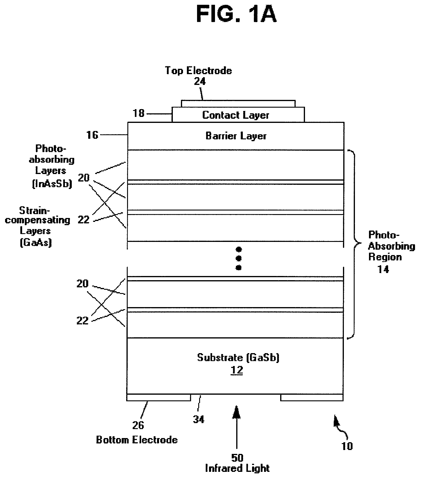
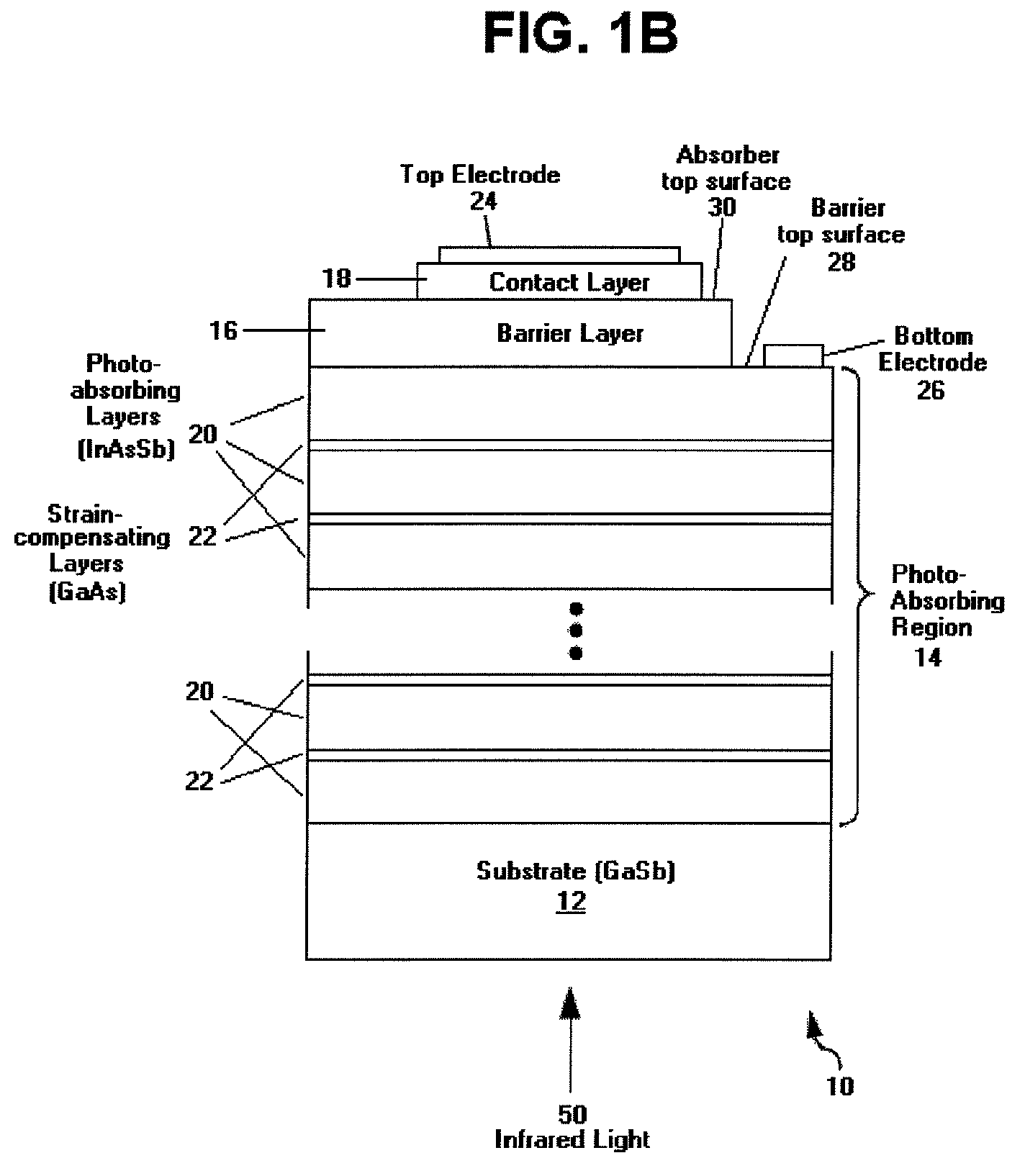
[0058]FIG. 1A shows a schematic cross-section view of an exemplary embodiment of a photodetector 10 of the present invention. Photodetector 10 comprises a semiconductor substrate 12 on which a plurality of III-V compound semiconductor layers are epitaxially grown to form a photo-absorbing region 14, a barrier layer 16, and a contact layer 18. The photo-absorbing region 14 (i.e. absorber, photo-absorber, absorber layer) comprises a plurality of strain-compensating layers 22 which are alternatingly interspersed between a plurality of photo-absorbing layers 20. In addition, a top electrode 24 is located above the contact layer 18 and a bottom e...


PUM


Abstract

A strain-balanced photodetector is provided for detecting infrared light at an extended cutoff wavelength in the range of 4.5 μm or more. An InAsSb absorber layer has an Sb content is grown in a lattice-mismatched condition to a GaSb substrate, and a plurality of GaAs strain-compensating layers are interspersed within the absorber layer to balance the strain of the absorber layer due to the lattice mismatch. The strain-compensation layers allow the absorber to achieve a thickness exhibiting sufficient absorption efficiency while extending the cutoff wavelength beyond that possible in a lattice-matched state. Additionally, the strain-compensation layers are sufficiently thin to be substantially quantum-mechanically transparent such that they do not substantially affect the transmission efficiency of the absorber. The photodetector is preferably formed as a majority carrier filter photodetector exhibiting minimal dark current, and may be provided individually or in a focal plane array.

Description

FIELD OF THE INVENTION[0001]The present invention relates in general to photodetectors, and in particular to infrared photodetectors with a majority carrier filter structure.BACKGROUND OF THE INVENTION[0002]A photodetector sensitive to the infrared wavelengths of light is also known as an infrared detector. Infrared detectors are used in a wide variety of applications, and in particular are used as thermal detection for surveillance, tracking, night vision, search and rescue, non destructive testing and gas analysis. Typically, an infrared detector is formed as a device consisting of an array, usually rectangular, of infrared light-sensing photodetectors disposed at the focal plane of an imaging lens. Such a detector is commonly referred to as a focal plane array (FPA).[0003]Infrared covers a broad range of wavelengths, and many materials are only sensitive to a certain range of wavelengths. As a result, the infrared band is further divided into sub-bands such as near infrared defin...

Claims


Application Information

Patent Timeline
Patent Type & Authority Patents(United States)
IPC IPC(8): H01L31/00
CPCH01L31/035236B82Y20/00H01L31/1844H01L31/0304H01L31/184H01L31/03046Y02E10/544H01L31/1035H01L27/142H01L27/14649H01L31/0232H01L33/14H01L33/30
Inventor SCOTT, JEFFREY W.PALOCZI, GEORGE
Owner LOCKHEED MARTIN CORP
Why Eureka
Try Eureka