
Strain compensated high electron mobility transistor

Inactive Publication Date: 2007-03-08
RAYTHEON CO
View PDF19 Cites 12 Cited by
  • Summary
  • Abstract
  • Description
  • Claims
  • Application Information

AI Technical Summary

Benefits of technology

[0004] In the pseudomorphic HEMT, the undoped gallium arsenide channel layer is replaced by a channel layer comprised of a lower bandgap material, such as gallium indium arsenide. Indium arsenide has a lattice constant α=6.0584. Since indium arsenide has a substantially different lattice constant compared to either gallium arsenide or aluminum arsenide, indium incorporation provides a crystal having a lattice constant which is substantially larger than the lattice constant of gallium arsenide or gallium aluminum arsenide. This lattice mismatch makes practical growth of such devices difficult and otherwise limits several advantages which would accrue to a device using GaInAs as the channel layer. For example, the use of gallium indium arsenide in a HEMT provides several performance advantages over gallium arsenide. Since gallium indium arsenide has a smaller bandgap than gallium arsenide, the conduction band discontinuity at the gallium aluminum arsenide / gallium indium arsenide heterojunction is increased thereby increasing the charge density transferred into the channel layer. Moreover, gallium indium arsenide also has a higher electron mobility and higher electron saturated velocity than gallium arsenide. Each of these benefits thus provides a pseudomorphic HEMT which can handle higher power levels, as well as, operate at higher frequencies with improved noise properties than a HEMT using gallium arsenide as the channel layer. Moreover, these benefits increase with increasing indium concentration (X) in the Ga1−xInx As layer.
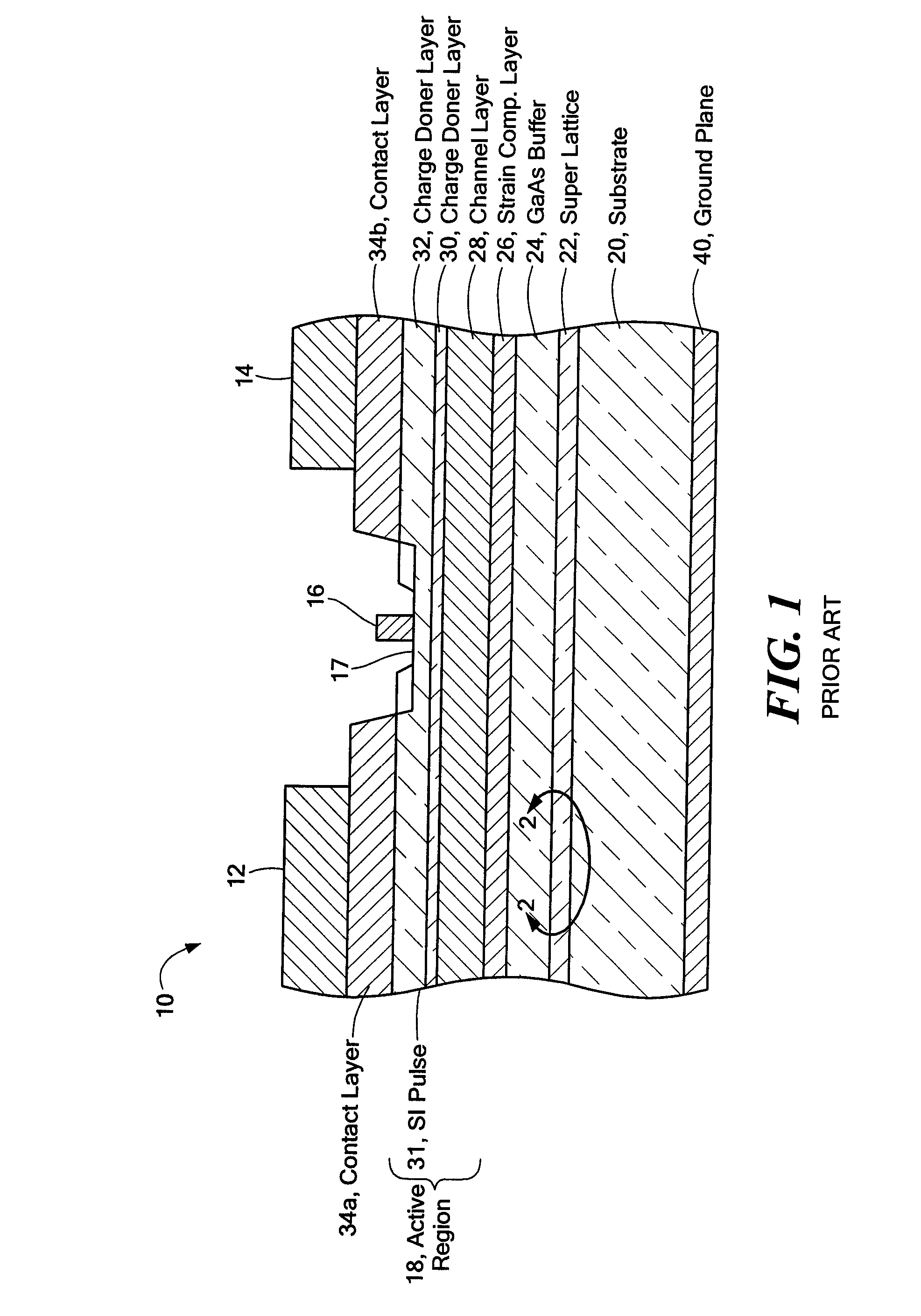
[0006] An example of a PHEMT structure is shown in FIG. 1. A key layer in the structure is the channel layer 28. In a pseudomorphic HEMT, the channel layer would be InGaAs which has a smaller bandgap than GaAs which, in turn, is smaller than AlGaAs. The charge donor layer 30, often AlGaAs, has a conduction band energy greater than the channel layer. The barrier layer is also a charge donor layer containing silicon dopant atoms. (FIG. 1 shows pulse doping but uniform doping can be used as well.) Electrons donated by the silicon atoms in the barrier fall into the channel layer well. This separation of the electrons from the donating silicon atoms increases the electron mobility and saturated velocity. Furthermore InGaAs has a higher mobility and peak saturated velocity than either GaAs or AlGaAs enhancing microwave and millimeter-wave operation.

Problems solved by technology

This conduction band discontinuity results in electrons leaving the donor barrier layer and entering the channel layer.
Thus due to resulting lattice constant mismatch the crystal structure of the material forming the channel layer is strained.
This lattice mismatch makes practical growth of such devices difficult and otherwise limits several advantages which would accrue to a device using GaInAs as the channel layer.
A problem arises, however, in increasing indium concentration.
The presence of such crystal dislocations seriously degrades the electron transport properties of the GaInAs layer.
Layers thinner than approximately 70 Angstroms are not attractive due to the increased importance of the quantum size effect which reduces the effective conduction band discontinuity.
Thicknesses much above 100 Angstroms result in the above-mentioned lattice dislocation problem.

Method used


Image

  • Strain compensated high electron mobility transistor
  • Strain compensated high electron mobility transistor
  • Strain compensated high electron mobility transistor

Examples


Embodiment Construction

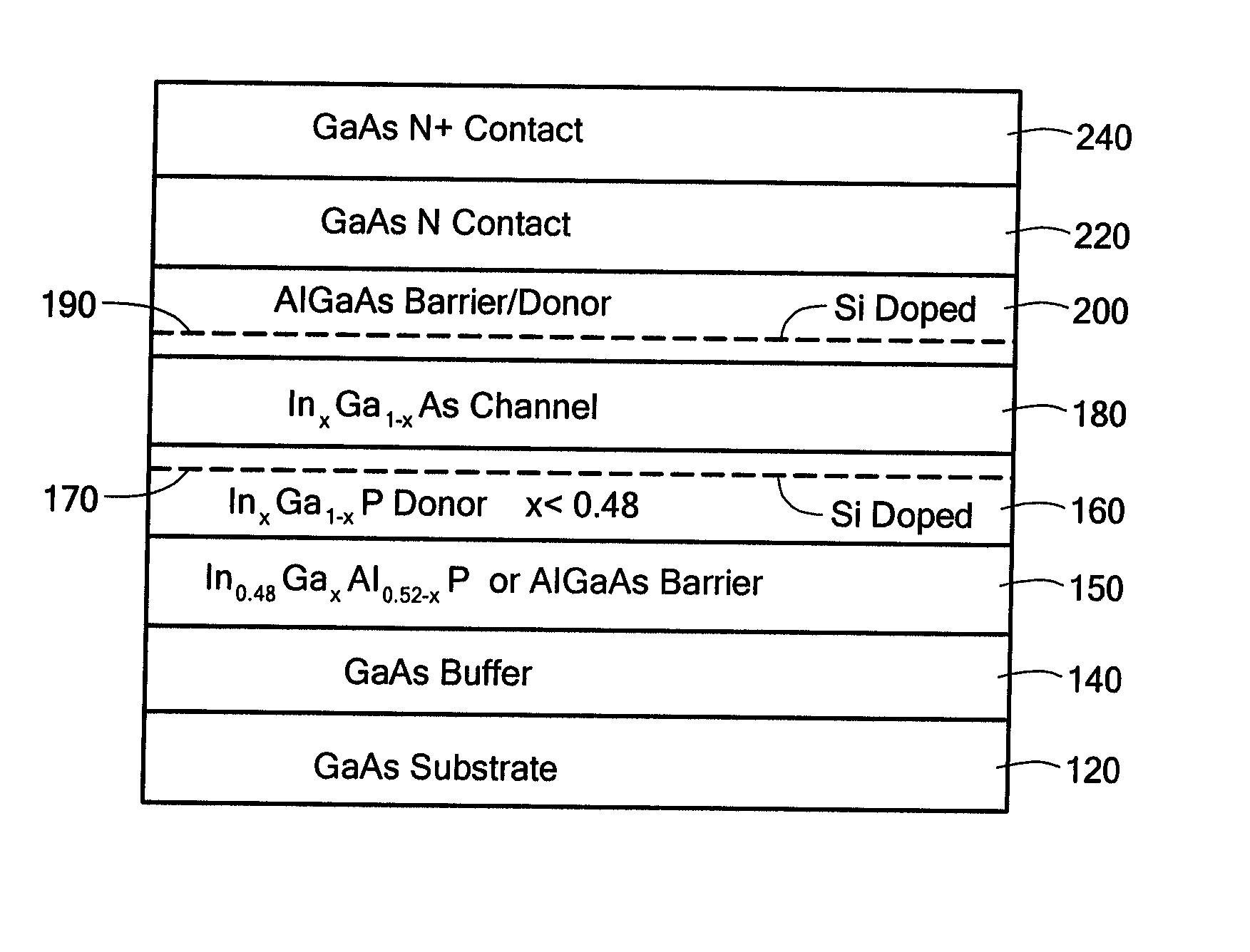
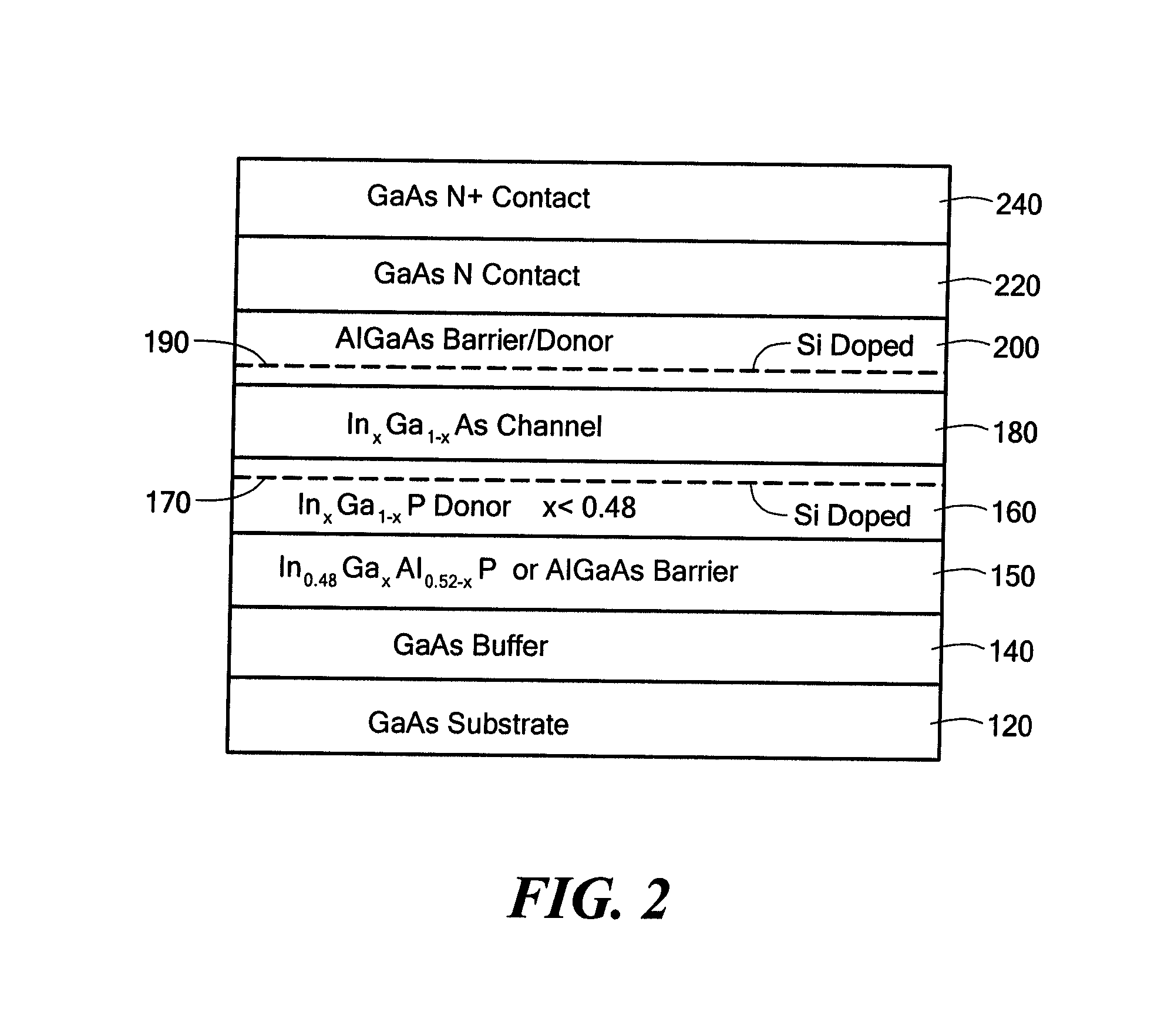
[0014] Referring now to FIG. 2, a semiconductor structure 100 is shown having: a III-V substrate 120, here GaAs; a buffer layer 140, here GaAs on the substrate 120; barrier layer 150, lattice matched to the GaAs buffer layer 140 and substrate 120, here, for example, In0.48GaxAl0.52−xP, and / or AlGaAs; a first III-V donor layer 160, here shown as InxGa1−xP with x less than 0.48, and having a relatively wide bandgap disposed on the buffer layer 140; a III-V channel layer 180, here InxGa1−xAs, where 0160, having a relatively narrow bandgap; a second III-V donor layer 200, here shown as AlGaAs, disposed on the channel layer 180. The donor layers have relatively large bandgaps such that the conduction band energy is greater in the donor layers than in the channel layer resulting in charge transfer from the donor layers to the channel layer. The first III-V donor layer 160 provides both tensile strain to compensate compressive strain in the channel layer 180 and charge carriers to the chan...


PUM


Abstract

A semiconductor structure having a III-V substrate; a first III-V donor layer having a relatively wide bandgap disposed over the substrate; a III-V channel layer having a relatively narrow bandgap disposed on the donor layer; a second III-V donor layer disposed on the channel layer having a relatively wide bandgap. The first III-V donor provides both tensile strain to compensate compressive strain in the channel layer and carriers to the channel layer.

Description

TECHNICAL FIELD [0001] This invention relates generally to high electron mobility transistors (HEMTs) and more particularly to HEMTs having strain compensation. BACKGROUND AND SUMMARY [0002] As is known in the art, there are several types of field effect transistors (FETs) generally used at microwave and millimeter wave frequencies. These FETs include metal semiconductor field effect transistors (MESFETs) and high electron mobility transistors (HEMTs), each fabricated from Group III-V materials. What distinguishes a HEMT from a MESFET is that in a HEMT charge is transferred from a doped charge donor layer to an undoped channel layer. The interface between the donor barrier layer and the channel layer is called a heterojunction. At the heterojunction, the conduction band is at a higher energy in the donor barrier layer than in the channel layer. This conduction band discontinuity results in electrons leaving the donor barrier layer and entering the channel layer. In most heterojuncti...

Claims


Application Information

Patent Timeline
IPC IPC(8): H01L27/14
CPCH01L29/7785
Inventor HOKE, WILLIAM E.
Owner RAYTHEON CO
Learn More