Castle-like chop mask for forming staggered datalines for improved contact isolation and pattern thereof

a technology of datalines and chop masks, applied in semiconductor devices, semiconductor/solid-state device details, electrical apparatus, etc., can solve the problems of increasing both processing time and cost of devics, short circuits, etc., to avoid short circuits, reduce resistance, and improve conductivity

Active Publication Date: 2014-03-18
NAN YA TECH
View PDF3 Cites 9 Cited by
  • Summary
  • Abstract
  • Description
  • Claims
  • Application Information

AI Technical Summary

Benefits of technology

[0008]A protect or periphery protect mask is a mask used during photolithography steps to prevent loop ends of spacers to be transferred to underlying substrates during etching. The castle-like shaped mask enables the formation of a staggered pattern of word lines that are alternatively shorter and longer. The staggered word lines pattern leaves a larger area for bigger contacts to be formed, which are also farther from one another, thereby avoiding short circuits and reducing their resistance for better conducting properties.
[0009]In ano

Problems solved by technology

The miniaturization however raises a problem of short circuits occurring when the contacts formed down to word lines are too close in proximity to adjac

Method used


Image

  • Castle-like chop mask for forming staggered datalines for improved contact isolation and pattern thereof
  • Castle-like chop mask for forming staggered datalines for improved contact isolation and pattern thereof
  • Castle-like chop mask for forming staggered datalines for improved contact isolation and pattern thereof

Examples


first embodiment

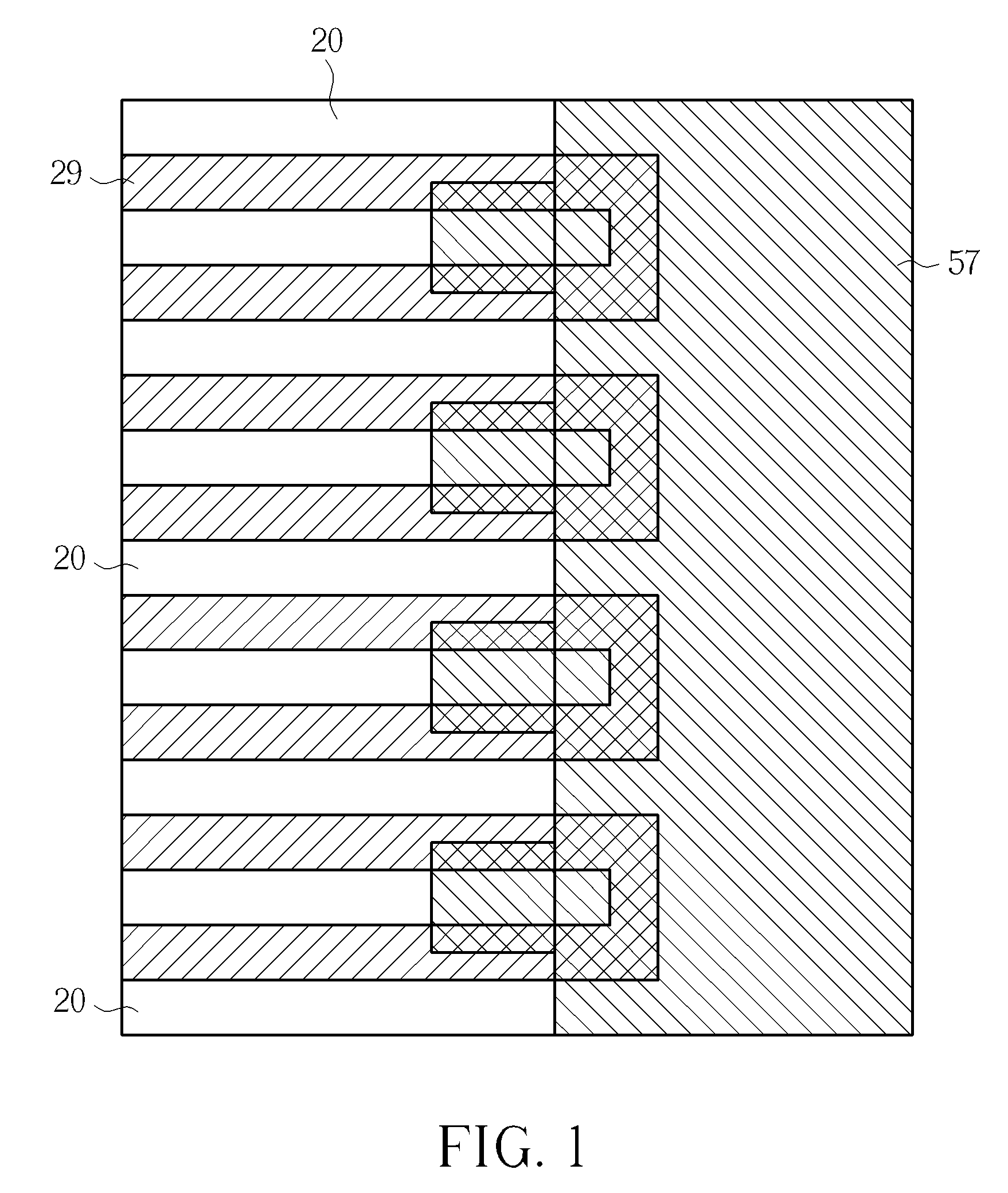
[0020]Please refer to FIGS. 1 and 2. FIGS. 1 and 2 are top views of a protect or periphery protect mask 57 according to the present invention. First, a substrate layer 10 is provided with a stack of materials 20 that may include carbon, DARC (Dielectric Anti Refracting Coating), etc. . . . , which are used in the formation of the word line pattern. The spacer pattern 29 is then formed on top of the substrate stack 20, by ways of pitch doubling or pitch multiplication techniques. The resulting spacer pattern 29 contains loop ends at the array edge. The protect or periphery protect mask 57 has a castle-like shape as a reference to castle battlements shapes, i.e. the protect or periphery protect mask is designed with a succession of squared parts regularly protruding from the main layer of the mask that have a width designed such that the resist edge will snap or self align to the spacer pattern 29. The chop mask 57 is disposed on the array edge of the spacers 29 so that the battlement...

second embodiment

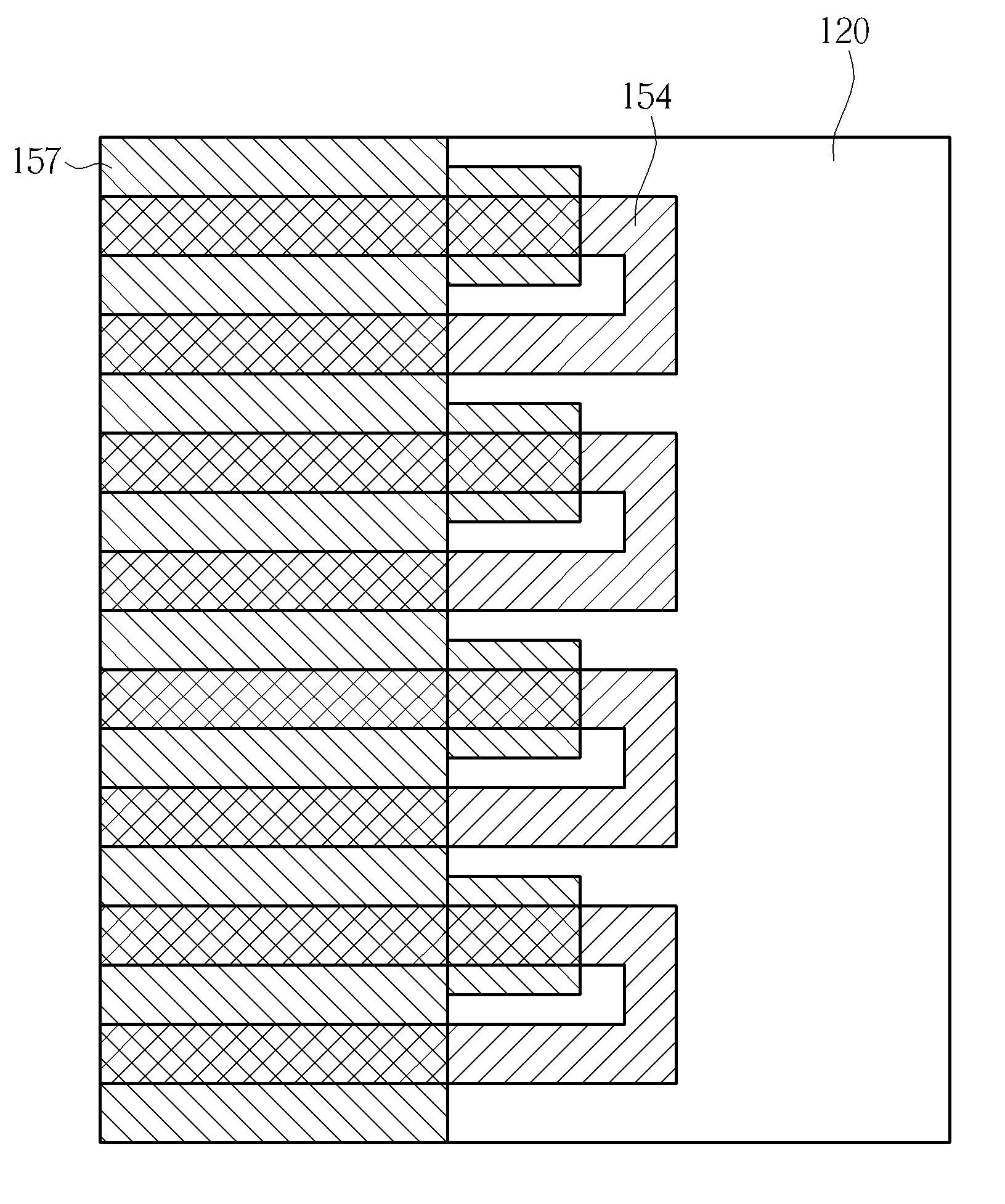
[0022]Please refer to FIGS. 5 and 6. FIGS. 5 and 6 are top views of a castle-like shaped DC chop mask 157 according to the present invention. First, a substrate layer 100 is provided with a stack of materials 120 that may include carbon, DARC, etc. . . . , which are used in the formation of the digit line pattern. The spacer pattern 154 is then formed on top of the substrate stack 120, by ways of pitch doubling or pitch multiplication techniques. The resulting spacer pattern 154 contains loop ends at the array edge. The DC chop mask 157 has a castle-like shape as a reference to castle battlements shapes, i.e. the DC chop mask is designed with a succession of squared parts regularly protruding from the main layer of the mask that have a width designed such that the resist edge snaps or self align to the spacer pattern 154. The DC chop mask is disposed on the array edge of the spacers 154 so that the castle battlement shaped protruding parts of the DC chop mask 157 are disposed corres...

third embodiment

[0025]Please refer to FIGS. 9 and 10. FIGS. 9 and 10 are top views of a DC chop mask 257 according to the present invention. First, a substrate layer 200 is provided with a stack of materials 220 that may include carbon, DARC, etc. . . . , which are used in the formation of the digit line pattern. The spacer pattern 254 is then formed on top of the substrate stack 220, by ways of pitch doubling or pitch multiplication techniques. The resulting spacer pattern 254 contains loop ends at the array edge. The DC chop mask 257 has a castle-like shape similar to the one of the previous embodiment, but with an additional part disposed perpendicularly to the end the protruding part, having the same width as the protruding part, and with a length slightly shorter than the part of the spacer loop that is parallel to the edge of the array. The DC chop mask 257 is disposed on the array edge of the spacers 254 so that the castle battlement shaped protruding parts of the DC chop mask 257 are dispos...


PUM


Abstract

The present invention provides a castle-like shaped protect or a periphery protect or a DC chop mask for forming staggered data line patterns in semiconductor devices so as to shift the adjacent data lines from one another so as to print contacts with larger areas at one end of each data line.

Description

BACKGROUND OF THE INVENTION[0001]1. Field of the Invention[0002]The present invention generally relates to a device pattern used in a semiconductor process and more precisely to a specific pattern allowing better contacts in a memory device and the mask to form such pattern.[0003]2. Description of the Prior Art[0004]With the trend of miniaturization of the semiconductor devices, word lines and bit lines in memory devices are closer to each other. The development of double patterning techniques have enabled smaller pitches to be obtained. Data lines need to be contacted to the rest of the IC circuit components to enable the transfer of data signal through contact plugs and landing pads.[0005]The miniaturization however raises a problem of short circuits occurring when the contacts formed down to word lines are too close in proximity to adjacent contacts or word lines, or efficiency problems when the contacts are too small. In prior art, specific plugs and landing pads formed through ...

Claims


Application Information

Patent Timeline
IPC IPC(8): H01L47/00
CPCH01L21/0337H01L21/32139H01L27/10885H01L27/10888H01L27/10891H10B12/482H10B12/488H10B12/485
Inventor PRATT, DAVIDHOUSLEY, RICHARD
Owner NAN YA TECH
Why Eureka
Try Eureka