SOI FinFET with recessed merged fins and liner for enhanced stress coupling

a technology of enhanced stress coupling and fins, which is applied in the direction of transistors, semiconductor devices, electrical equipment, etc., can solve the problems of unsuitable real-time technology of shang claims, and achieve the effects of improving device performance, reducing spreading resistance, and improving stress transfer to the channel

Active Publication Date: 2014-05-13
GLOBALFOUNDRIES US INC
View PDF24 Cites 5 Cited by
  • Summary
  • Abstract
  • Description
  • Claims
  • Application Information

AI Technical Summary

Benefits of technology

[0020]An advantage of the recessed epi-merge layer is that the closer proximity of the liner to the channel results in improved stress transfer to the channel and improves the device performance as compared to non-recessed 3D devices. A further advantage of the recessed epi-merge region is that a vertical silicide is formed in the plane of the channel thus reducing spreading resistance. An additional advantage is that by forming dummy spacers after source / drain ion implantation, the gate is shielded from possible silicide encroachment to minimize the possibility of shorting the gate. In yet another advantage, the effective switching capacitance (Ceff) is reduced due to the lower PC-to-epi fringe capacitances.

Problems solved by technology

Previous demonstrations use large S / D landing pads for a simplified contact scheme which Shang claims is unsuitable for a realistic technology.

Method used


Image

  • SOI FinFET with recessed merged fins and liner for enhanced stress coupling
  • SOI FinFET with recessed merged fins and liner for enhanced stress coupling
  • SOI FinFET with recessed merged fins and liner for enhanced stress coupling

Examples


Embodiment Construction

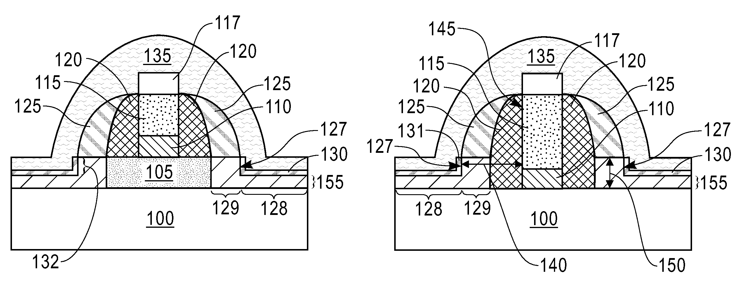
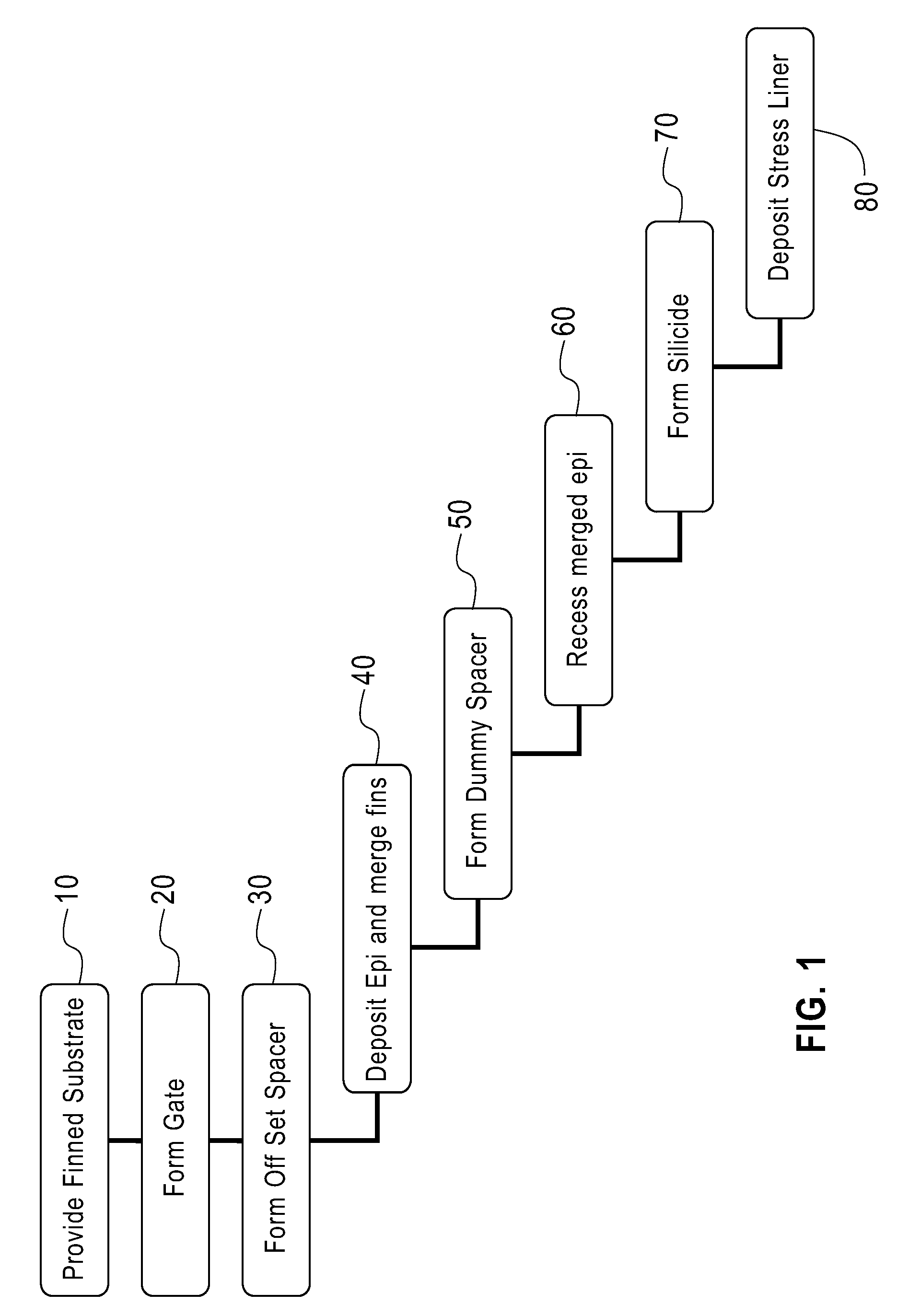
[0043]The basic principle of the invention is a method for creating a high performance FinFET by recessing an epi-merge region and forming a stress liner over the merged region and gate stack. The method will be described in conjunction with FIGS. 1-8. The invention also includes a structure of a FinFET having an epi-merge field area which is recessed, an epi-merge spacer area, and an optional vertical silicide which is perpendicular to the substrate. In addition to the earlier figures, the structure will be further described in conjunction with FIGS. 9-10. A detailed description of the invention is made in combination with the following embodiments. Please note that reference numbers are merely reference numbers and, thus, do not necessarily restrict the method to the numerical order of the reference numbers.

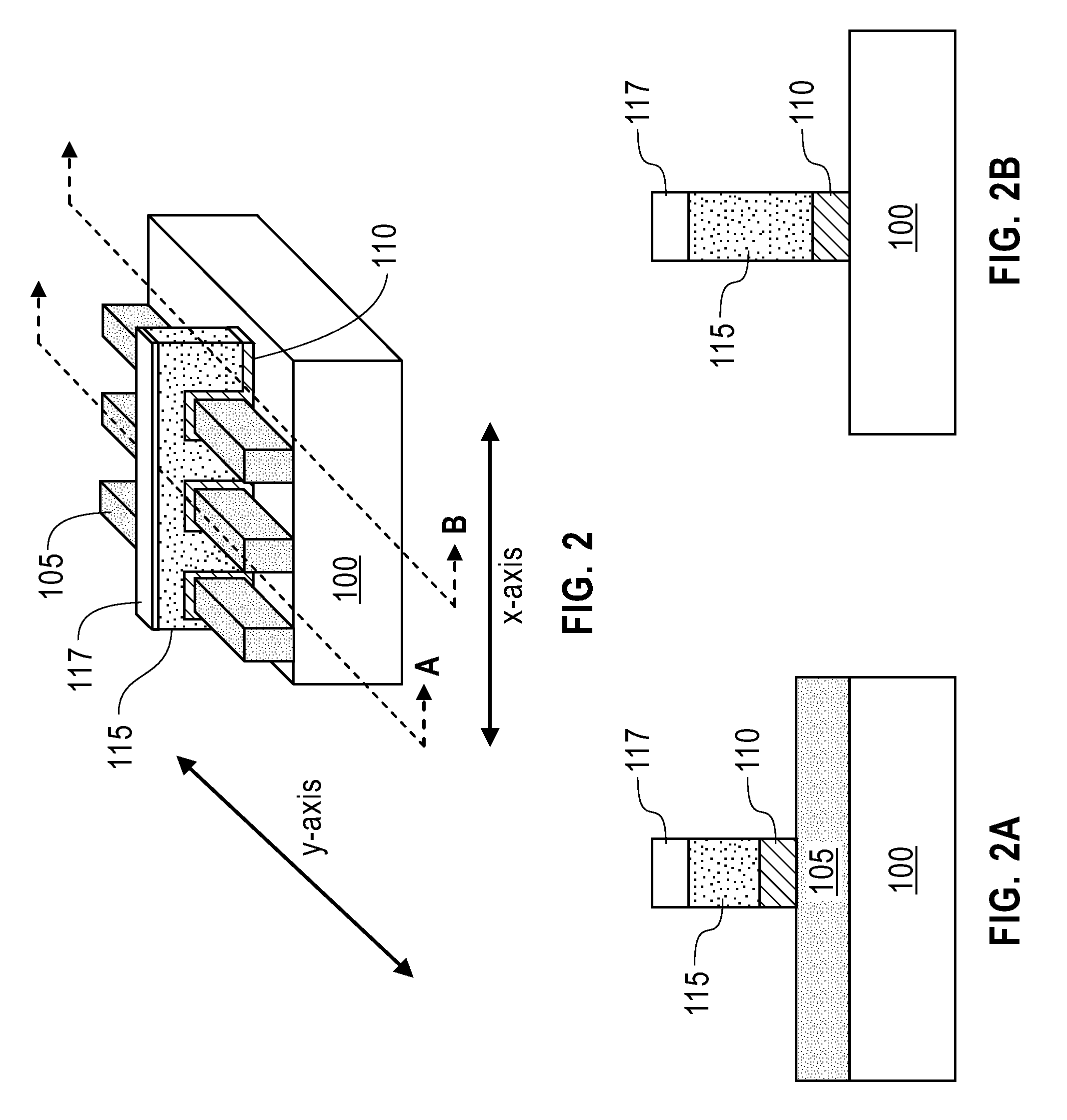
[0044]FIG. 1 is a flow chart with method steps of creating a high performance FinFET with a recessed epi-merge field region according to an embodiment of the invention. Step 10...


PUM


Abstract

FinFETS and methods for making FinFETs with a recessed stress liner. A method includes providing an SOI substrate with fins, forming a gate over the fins, forming an off-set spacer on the gate, epitaxially growing a film to merge the fins, depositing a dummy spacer around the gate, and recessing the merged epi film. Silicide is then formed on the recessed merged epi film followed by deposition of a stress liner film over the FinFET. By using a recessed merged epi process, a MOSFET with a vertical silicide (i.e. perpendicular to the substrate) can be formed. The perpendicular silicide improves spreading resistance.

Description

CROSS-REFERENCE TO RELATED APPLICATION[0001]This application is a continuation of U.S. patent application Ser. No. 13 / 330,746, filed Dec. 20, 2011, now U.S. Pat. No. 8,445,334, the disclosure of which is incorporated by reference herein in its entirety.BACKGROUND OF THE INVENTION[0002]1. Field of the Invention[0003]The present invention generally relates to a non-planar Metal Oxide Semiconductor Field Effect Transistors (MOSFETs) made on semiconductor on insulator (SOI) substrates wherein the MOSFET has a stress enhancement layer. In particular, the invention relates to FinFETs with a merged source drain region in which the merged region is recessed and a stress adjustment layer which is deposited over the source drain region and a gate stack of the FinFET.[0004]2. Description of Related Art[0005]In a paper entitled “A 90 nm High Volume Manufacturing Logic Technology Featuring Novel 45 nm Gate Length Strained Silicon CMOS Transistors,” by T. Ghani et al. in IEDM 2003 a nitride layer...

Claims


Application Information

Patent Timeline
Patent Type & Authority Patents(United States)
IPC IPC(8): H01L31/0392H01L27/12H01L27/01
CPCH01L21/00H01L29/7843H01L29/6656H01L29/66795H01L27/088
Inventor BASKER, VEERARAGHAVAN S.BU, HUIMINGLEOBANDUNG, EFFENDISTANDAERT, THEODORUS E.YAMASHITA, TENKOYEH, CHUN-CHEN
Owner GLOBALFOUNDRIES US INC
Why Eureka
Try Eureka