Light emitting module and illumination apparatus

a technology illumination apparatuses, which is applied in the direction of lighting and heating apparatus, instruments, semiconductor devices for light sources, etc., to achieve the effects of reducing costs, facilitating the mounting of light emitting diode elements on the module substrate, and improving the manufacturing efficiency of light emitting modules

Inactive Publication Date: 2014-07-08
TOSHIBA LIGHTING & TECH CORP
View PDF15 Cites 2 Cited by
  • Summary
  • Abstract
  • Description
  • Claims
  • Application Information

AI Technical Summary

Benefits of technology

[0043]According to the light emitting module of claim 4, the die bond material interposed between the light emitting diode elements and the metal reflective layer has lower gas permeability than the sealing member and protrudes around the light emitting diode elements. Therefore, even if, e.g., a corrosive gas permeates the sealing member, the corrosive gas that has permeated the sealing member is hard to reach positions associated with the light emitting diode elements and a region surrounding the periphery of the light emitting diode elements in the metal reflective layer. Therefore, discoloration of the metal reflective layer due to the corrosive gas is suppressed, thereby excellently maintaining light reflection properties of the metal reflective layer.
[0044]The die bond material having the low gas permeability unavoidably becomes harder than the sealing member. However, the hard die bond material is apart from each bonding wires of the light emitting diode string. Therefore, even if the die bond material thermally expands or contracts based on a heat cycle, the die bond material does not function as a factor that stresses the bonding wires.
[0045]In the light emitting module according to claim 5, the sealing member is made of a softer resin material than the die bond material. If the sealing member is soft, stress applied to the bonding wires by the sealing member can be reduced even though the sealing member thermally expands or contracts based on the heat cycle.
[0046]In the light emitting module according to claim 6, the die bond material contains a phenyl silicone component. The phenyl silicone resin has lower gas permeability than, e.g., dimethyl silicone resin. Therefore, the die bond material containing the phenyl silicone component prevents the metal reflective layer from being exposed to a gas that has permeated the sealing member.
[0051]According to the illumination apparatus of claim 9, heat of the light emitting diode elements transmitted to the module substrate of the light emitting module is transferred to the heat sink from the module substrate through the heat receiving portion. Therefore, the main body of the illumination apparatus can be utilized to improve the thermal radiation properties of the light emitting module.
[0052]According to the light emitting module of claim 1, under the conditions that the space in the direction along which the light emitting diode string extends is limited, the light emitting diode elements can be highly densely arranged on the module substrate. Further, it is good enough to supply the light emitting diode elements onto the module substrate in the state that directions of the element electrodes with the same polarity are uniformed. Therefore, directions of the light emitting diode elements do not have to be alternately reversed, the work of mounting the light emitting diode elements on the module substrate can be facilitated. Furthermore, since the bonding wires are arranged according to a given rule, whether implementation of the bonding wires has a defect can be recognized at first sight. Therefore, the light emitting module manufacturing efficiency can be improved to reduce a cost.
[0053]According to the light emitting module of claim 2, strength of the bonding wires can be enhanced to avoid undesired damage and disconnection of the bonding wires. Moreover, voids that scatter light hardly remains in the sealing member put between the light emitting diode elements adjacent to each other, thus obtaining appropriate distribution of light.
[0054]According to the light emitting module of claim 3, even if the sealing member thermally expands or contract, stress applied to the bonding wires by the sealing member can be reduced.
[0055]According to the light emitting module of claim 4, thermal radiation properties of the light emitting diode elements can be improved to excellently maintain the light emission efficiency of the light emitting diode elements. Additionally, discoloration of the light reflecting surface of the metal reflective layer due to a gas that has permeated the sealing member can be suppressed to excellently maintain light reflection performance of the metal reflective layer, thereby increasing light extraction efficiency.
[0056]According to the light emitting module of claim 5, even if the sealing member thermally expands or contract, stress applied to the bonding wires by the sealing member can be alleviated. Therefore, reliability of electrical connection between the bonding wires and the light emitting diode elements can be assured.
[0057]According to the light emitting module of claim 6, the gas flowing from the die bond material to the metal reflective layer can be assuredly blocked, thereby avoiding deterioration of the light reflection performance involved by corrosion of the metal reflective layer.
[0058]According to the light emitting module of claim 7, since the gas hardly permeate both the sealing member and the die bond material, corrosion and deterioration in the light reflection performance of the metal reflective layer can be assuredly avoided.
[0059]According to the illumination apparatus of claim 8, the light emitting module having the improved manufacturing efficiency can be used as a light source, a manufacturing cost of the illumination apparatus can be reduced, and the inexpensive illumination apparatus can be provided.
[0060]According to the illumination apparatus of claim 9, the thermal radiation properties of the light emitting module can be improved, and a reduction in light emission efficiency involved by overheating of the light emitting module can be prevented.

Problems solved by technology

Therefore, in the illumination apparatus described in Patent Literature 1, when a space in the direction along which the light emitting diode string extends is limited, there occurs the following problem.

Method used


Image

  • Light emitting module and illumination apparatus
  • Light emitting module and illumination apparatus
  • Light emitting module and illumination apparatus

Examples


first embodiment

[0077]A first embodiment according to the present invention will now be described hereinafter with reference to FIG. 1 to FIG. 8.

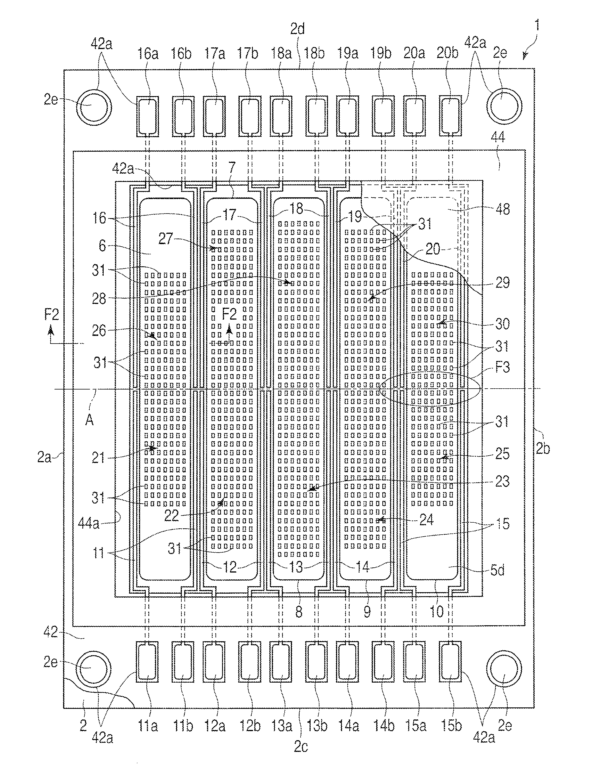
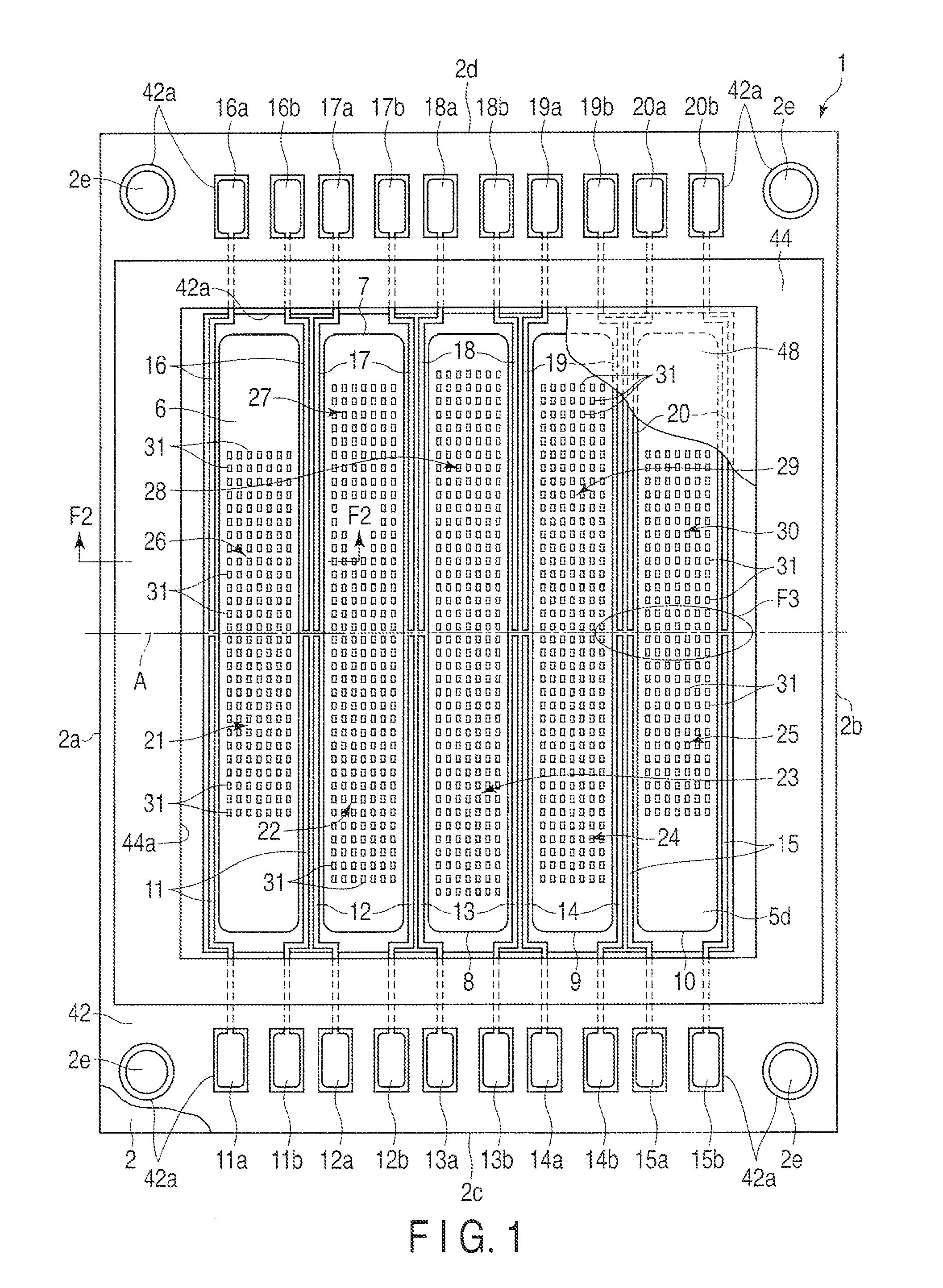
[0078]FIG. 1 and FIG. 2 disclose a chip-on-a-board (COB) light emitting module 1. The light emitting module 1 is arranged on a focal point of a projector lens group of, e.g., a spotlight and used as a light source of the spotlight.

[0079]The light emitting module 1 comprises a module substrate 2 functioning as a base. As shown in FIG. 1, the module substrate 2 is formed into a rectangular shape having a pair of wide sides 2a and 2b and a pair of narrow sides 2c and 2d. The wide sides 2a and 2b are parallel to each other, and the narrow sides 2c and 2d are also parallel to each other. Further, the module substrate 2 has four corner portions. A fitting hole 2e is formed in each corner portion of the module substrate 2.

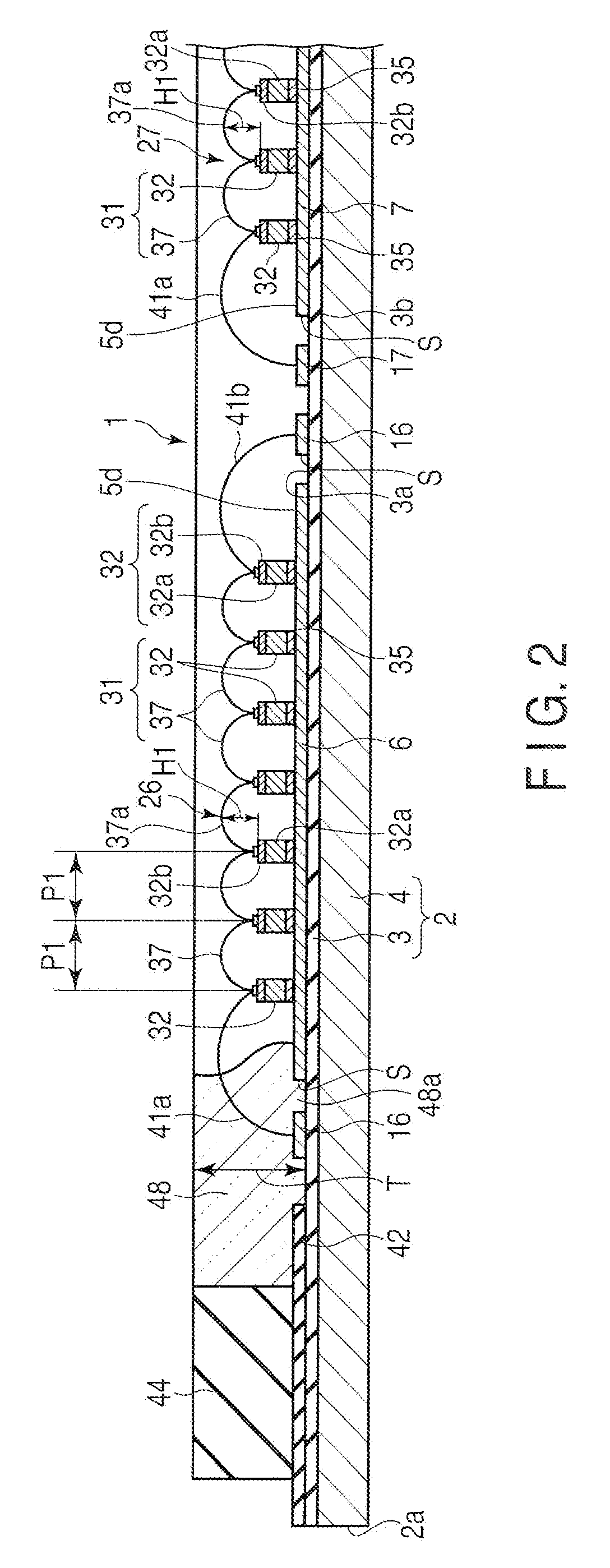
[0080]As shown in FIG. 2, the module substrate 2 is constituted of an insulating layer 3 made of synthetic resin and a metal plate 4. The insul...

second embodiment

[0171]FIG. 9 and FIG. 10 disclose a second embodiment according to the present invention.

[0172]The second embodiment is different from the first embodiment in particulars concerning the die bond materials that bonds the light emitting diode elements to the first to fifth metal reflective layers. A basic configuration of the light emitting modules excluding the die bond material is equal to that of the first embodiment. Therefore, in the second embodiment, like reference numerals denote constituent parts equal to those in the first embodiment, thereby omitting a description thereof.

[0173]As shown in FIG. 9 and FIG. 10, die bond materials 35 are applied to cover first to fifth metal reflective layers 6 to 10 and interposed between silver layers 5c and a substrate 32a of respective light emitting diode elements 32. The die bond material 35 covers an entire region of each silver layer 5c excluding side edge portions of this layer.

[0174]In other words, the die bond material 35 continuous...

third embodiment

[0191]FIG. 11 to FIG. 13 disclose a third embodiment according to the present invention.

[0192]The third embodiment is different from the first embodiment in particulars concerning the die bond materials that bonds light emitting diode elements to first to fifth metal reflective layers. A basic configuration of a light emitting module excluding the die bond materials is equal to that in the first embodiment. Therefore, in the third embodiment, like reference numerals denote constituent parts equal to those in the first embodiment, thereby omitting a description thereof.

[0193]FIG. 11 is a view associated with FIG. 3 of the first embodiment and mainly shows a state of fifth and tenth light emitting portions 25 and 30 bonded to an upper side of a fifth metal reflective layer 10.

[0194]As shown in FIG. 11, a die bond material 35 that bonds light emitting diode elements 32 of light emitting diode strings 31 to a light reflecting surface 5d of the fifth metal reflective layer 10 has a plura...


PUM

PropertyMeasurementUnit
heightaaaaaaaaaa
heightaaaaaaaaaa
heightaaaaaaaaaa

Abstract

A light emitting module (1) comprises a module substrate (2), a light emitting diode string (31), and a sealing member (48). The light emitting diode string (31) includes light emitting diode elements (32) and bonding wires (37) which connect the light emitting diode elements (32). The light emitting diode element (32) has a pair of element electrodes (33, 34) and has a rectangular shape extending in a direction along which the element electrodes (33, 34) are aligned. The sealing member (48) is laminated on the module substrate (2) to seal the light emitting diode string (31). The light emitting diode elements (32) are arranged at intervals in a direction crossing the direction along which the element electrodes (33, 34) are aligned, and the element electrodes (33, 34) with the same polarity are aligned to be adjacent to each other in an arrangement direction of the light emitting diode elements (32) between the light emitting diode elements (32) adjacent to each other. Each bonding wire (37) is obliquely wired with respect to the arrangement direction of the light emitting diode elements (32) to connect the element electrodes (33, 34) with different polarities of the light emitting diode elements (32) adjacent to each other.

Description

CROSS-REFERENCE TO RELATED APPLICATIONS[0001]This is a U.S. National Phase application under 35 USC 371 of International Application No. PCT / JP2010 / 053136 (not published in English), filed Feb. 26, 2010, which, in turn, claims the benefit of Japanese Patent Application Nos. 2009- 046739, filed on Feb. 27, 2009; 2009- 046740, filed on Feb. 27, 2009; 2009- 046741, filed on Feb. 27, 2009; and 2010-039563 filed on Feb. 25, 2010.TECHNICAL FIELD[0002]The present invention relates to a light emitting module having a plurality of light emitting diode elements. Furthermore, the present invention relates to an illumination apparatus that uses a light emitting module having a plurality of light emitting diode elements as a light source.BACKGROUND ART[0003]For example, Patent Document 1 discloses an illumination apparatus which is of a chip-on-a-board (COB) type. This kind of illumination apparatus includes a resin substrate having a white surface, a plurality of light emitting diode strings, a...

Claims


Application Information

Patent Timeline
Patent Type & Authority Patents(United States)
IPC IPC(8): G02F1/1335
CPCF21K9/00F21V29/004F21V29/2243F21V29/2262F21Y2101/02F21Y2105/001H01L25/0753H01L33/62H01L2224/45144H01L2224/48091H01L2224/48137F21V29/75F21V29/76F21Y2105/10F21Y2115/10Y10S362/80F21V29/70H01L2924/00014H01L2924/00H01L33/48H01L33/00
Inventor SANPEI, TOMOHIROOTANI, KIYOSHIIZUMI, MASAHIROMURATA, JUNYASAITO, AKIKOHAYASHIDA, YUMIKO
Owner TOSHIBA LIGHTING & TECH CORP
Why Eureka
Try Eureka