Conduction cooling of multi-channel flip chip based panel array circuits

a panel array circuit and flip chip technology, applied in the direction of electrical apparatus construction details, instruments, casings/cabinets/drawers, etc., can solve the problems of high power circuits, densely packed circuits, and insufficient air cooling for devices such as phased array antennas, so as to improve thermal performance, enhance thermal conductivity, and minimize thermal gaps

Active Publication Date: 2014-07-15
RAYTHEON CO
View PDF30 Cites 26 Cited by
  • Summary
  • Abstract
  • Description
  • Claims
  • Application Information

AI Technical Summary

Benefits of technology

[0016]It is advantageous, therefore, if techniques for thermal management can minimize the thermal gap, so as to enhance thermal conductivity, using a straightforward manufacturing process that produces high thermal performance, thus providing performance improvements (improved reliability, increase radiated power) over the prior art. The prior art configuration of FIG. 1, for example, results in thermal conductivity on the order of 1-2 Watts / meter / degree-Kelvin (W / m / ° K). In contrast, the techniques described in accordance with the inventive embodiments herein can provide thermal conductivities on the order of 20-40 W / m / ° K and greater.
[0017]As described herein, the invention provides several techniques and apparatus for minimizing thermal gap in flip chip MMIC packaging assemblies.
[0023]In a still further embodiment, the first and second thickness of the first and second thermal spreader materials are each constructed and arranged to minimize the thermal gap between the respective thermal spreader material, corresponding semiconductor IC chip, and substrate, to less than 2 mils. In another embodiment, the second surface of the first semiconductor IC chip has a first shape in the x and y plane and wherein the x and y dimensions of the corresponding first portion of first thermal spreader material are selected to either (a) substantially mate to the first shape or (b) have a shape selected to provide a predetermined thermal compensating effect to the first semiconductor IC chip.

Problems solved by technology

This air cooling can be insufficient, however, for high power circuits and / or densely packed circuits.
Providing sufficient cooling for devices such as phased array antennas can present challenges.
Although this approach may satisfy the cooling requirements for the active phased array, this approach to thermal management is limited to relatively low power density active phased array's because the temperature rise is the cooling air stream can result in excessive variations in temperature across the array which will negatively impact performance.
Removing heat from flip-chips, especially those in configurations such as panel arrays, can be difficult.
This thermal performance can be very limiting in some applications and limits the thermal performance of any module in which the flip chips 14 are a part, as well as the amount of power that could be used with such a module.
The gap-pad technique can result in a thermal path having poor bulk thermal conductivity.
Another issue with use of the thermal gap pad 18 of the prior art assembly 10 of FIG. 1 is that there can be a significant compression / clamping force required to form the thermal gap pad 18 around the flip chips 14 so as to minimize and / or reduce air gaps.
This high force can result in damage to the flip chips 14.
If an implementation uses a thermal gap pad, for example (as is done in the prior art), the thermal conductive path to the cooling manifold can be poor and can greatly compromise the thermal performance of the module as well as the amount of power that could be used with it.
A further issue with the use of the thermal gap pad 18 is that the compression of the thermal gap pad 18 attempts to compensate for variations in spacing between the surface of a heat dissipating member and a heat generating device.
Such variations in thickness can result in temperature gradients across the array of active circuits.
When the active circuits 14 and gap pad 18 are used as part of a phased array antenna, the phased array antenna will have temperature gradients, and such temperature gradients adversely affect the performance of the phased array antenna.
Designing an antenna of medium to high power density to meet this thermal gradient is a difficult problem to solve in a phased array radar.
However for packages that contain multiple flip chips of different thicknesses, and / or which can include radio frequency (RF) RF MMICs that require consistent temperatures be achieved from device to device, the mechanical tolerances of these devices (the RF MMICs) result in thermal gaps that are problematic for a thermally conductive epoxy to meet cooling requirements.
Consequently, the thickness of each printed wiring board (PWB) to which the flip chip is attached, and the relatively large tolerances associated with the PWB can present an additional thermal management problem, and can result in a total tolerance stackup of about + / −0.013″ (inches), which would require an unacceptably thick epoxy based thermal interface.
However this method has limitations should the ‘backside’ one or more flip chips be at electrical potential.
In this instance application of this method would result in an electrical short circuit.

Method used


Image

  • Conduction cooling of multi-channel flip chip based panel array circuits
  • Conduction cooling of multi-channel flip chip based panel array circuits
  • Conduction cooling of multi-channel flip chip based panel array circuits

Examples


Embodiment Construction

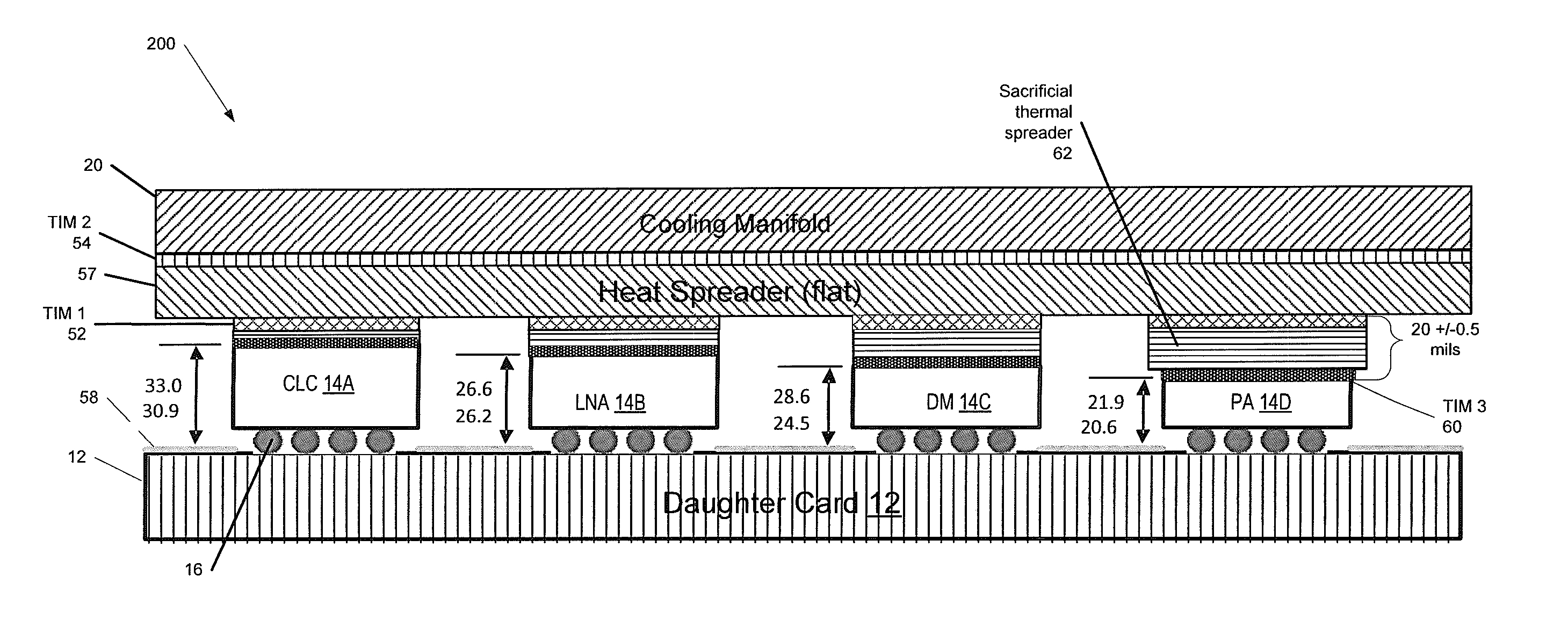
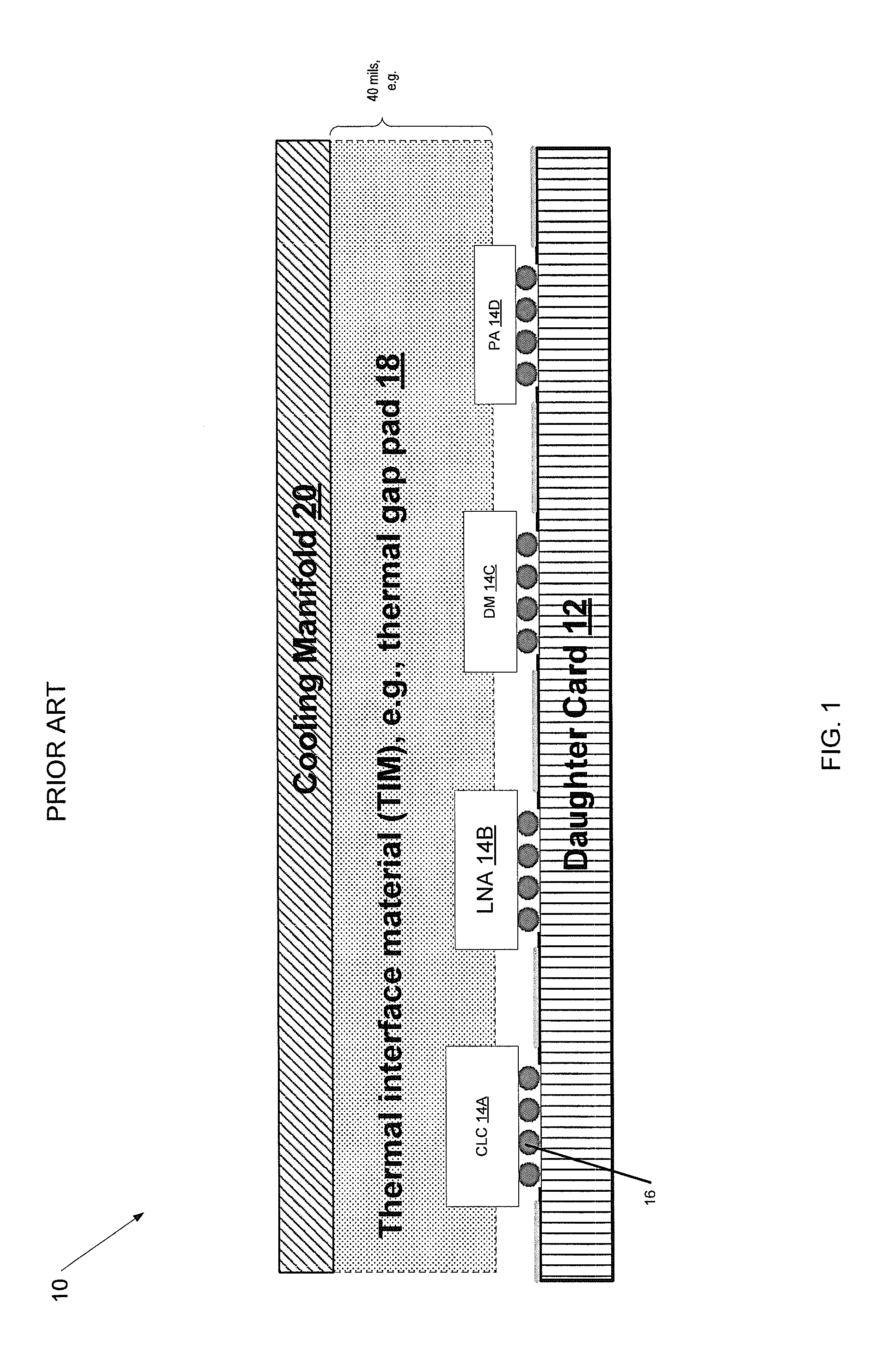
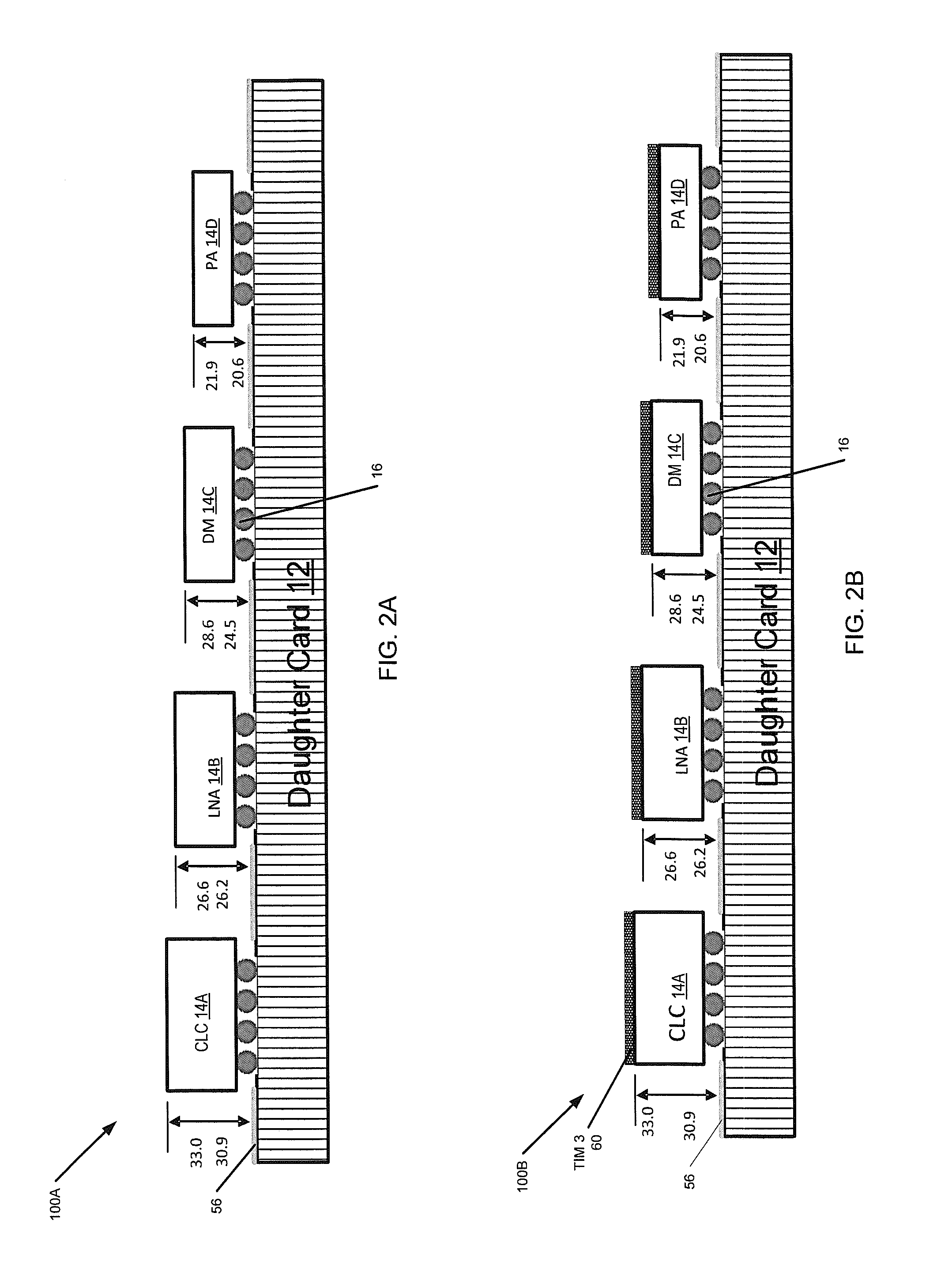
[0043]In addition to the various embodiment or embodiments disclosed below, this invention is capable of other embodiments and of being practiced or being carried out in various ways. For example, the invention is applicable to virtually any electrical device that has components that generate heat, have multiple planar surfaces that conduct this heat to one substantially planar heat sink and therefore is and is not limited to flip chip, MMICs, or active electronically scanned array (AESA) (also known as phased array) assemblies. At least some of the embodiments of the invention described herein have applicability to devices such as mobile computing devices, having one or more CPU chips, where use of liquid and / or fan cooling is impractical or impossible. Various embodiments of the invention include (but are not limited too), integrated microelectronics modules that feature multiple flip chips that engage one substantially planar heat sink, and the like.

[0044]Advantageously, the embo...


PUM

PropertyMeasurementUnit
total heightaaaaaaaaaa
poweraaaaaaaaaa
temperatureaaaaaaaaaa

Abstract

A method of forming a heat-dissipating structure for semiconductor circuits is provided. First and second semiconductor integrated circuit (IC) chips are provided, where the first and second semiconductor chips each have first and second opposing sides, wherein the first and second semiconductor IC chips are configured to be fixedly attached to a top surface of a substantially planar circuit board along their respective first sides. The respective second opposing sides of each of the first and second semiconductor IC chips are coupled to first and second respective portions of a sacrificial thermal spreader material, the sacrificial thermal spreader material comprising a material that is thermally conductive. The first and second portions of the sacrificial thermal spreader material are planarized to substantially equalize a respective first height of the first semiconductor chip and a respective second height of the second semiconductor chip.

Description

FIELD OF THE INVENTION[0001]Embodiments of the invention generally relate to improving the thermal performance of devices such as flip chip based panel arrays. More particularly, the invention relates to devices and methods for assembling flip chip based panel arrays with minimal thermal gaps between the flip chips and heat spreaders.BACKGROUND OF THE INVENTION[0002]As those of skill in the art are aware, many different techniques can be used to provide cooling of electrical components. For example, circulation of air within a housing can be sufficient to cool some types of electrical components contained within the housing. Some electrical assemblies further include physical features (e.g., cooling fins, cooling manifolds) that increase the surface area exposed to convective air currents, or provide fans to circulate the air further, providing further cooling. This air cooling can be insufficient, however, for high power circuits and / or densely packed circuits.[0003]High power and / ...

Claims


Application Information

Patent Timeline
Patent Type & Authority Patents(United States)
IPC IPC(8): H05K7/20H01L21/00H01L21/50
CPCH01L23/433H01L25/0655H01L2224/16225H01L2224/73253Y10T29/49126Y10T29/49146
Inventor DANELLO, PAUL A.STANDER, RICHARD A.GOULET, MICHAEL D.
Owner RAYTHEON CO
Why Eureka
Try Eureka