Semiconductor element having conductive vias and semiconductor package having a semiconductor element with conductive vias and method for making the same

a technology of conductive vias and semiconductor elements, which is applied in the direction of semiconductor devices, semiconductor/solid-state device details, electrical apparatus, etc., can solve problems such as interference with a redistribution layer, problems such as affecting product yield, and achieve the effect of raising at least one product yield ra

Active Publication Date: 2014-07-22
ADVANCED SEMICON ENG INC
View PDF123 Cites 26 Cited by
  • Summary
  • Abstract
  • Description
  • Claims
  • Application Information

AI Technical Summary

Benefits of technology

[0010]In the present invention, the difference between a first radius of each of the through holes and a second radius of the first central hole is substantially in a range from 5 to 19 μm, which prevents first metal pads covered on the first insulation layer from breaking or being overly thin, so an electrical connection between the conductive vias and the other element can be ensured. Moreover, the thickness of the silicon substrate is between 75 and 150 μm, so during a process of electrically connecting the silicon substrate of the present invention and the other semiconductor element, the shift of the silicon substrate caused by warpage of the silicon substrate during a heat process can be avoided, and the electrical connection between the silicon substrate and the chip can be ensured, so as to raise at least one yield rate of a product.

Problems solved by technology

However, problems can occur if the insulation layer is not the proper thickness.
For example, if the insulation layer is too thick, it may expand due to heat to such an extent that it interferes with a redistribution layer (RDL).
Furthermore, various problems can occur if the silicon substrate is not of an optimal thickness.

Method used


Image

  • Semiconductor element having conductive vias and semiconductor package having a semiconductor element with conductive vias and method for making the same
  • Semiconductor element having conductive vias and semiconductor package having a semiconductor element with conductive vias and method for making the same
  • Semiconductor element having conductive vias and semiconductor package having a semiconductor element with conductive vias and method for making the same

Examples


Embodiment Construction

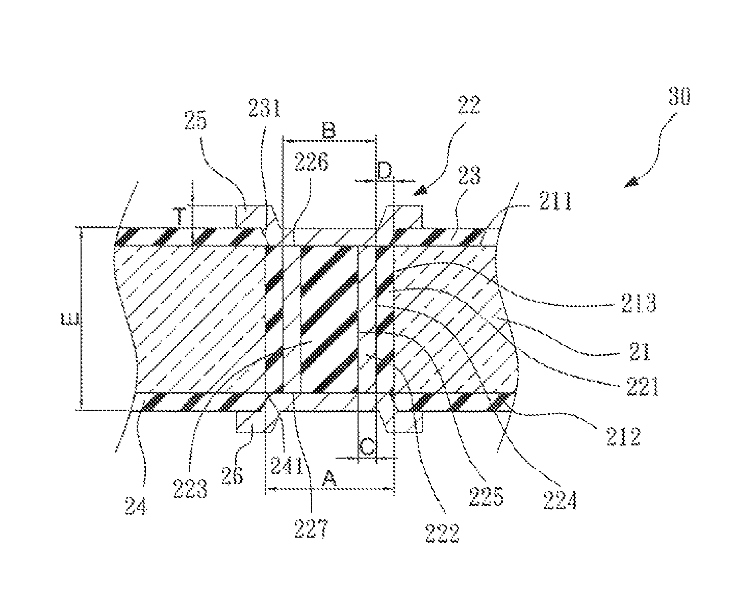
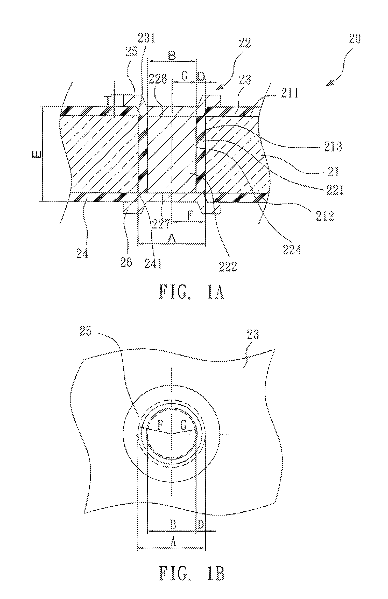
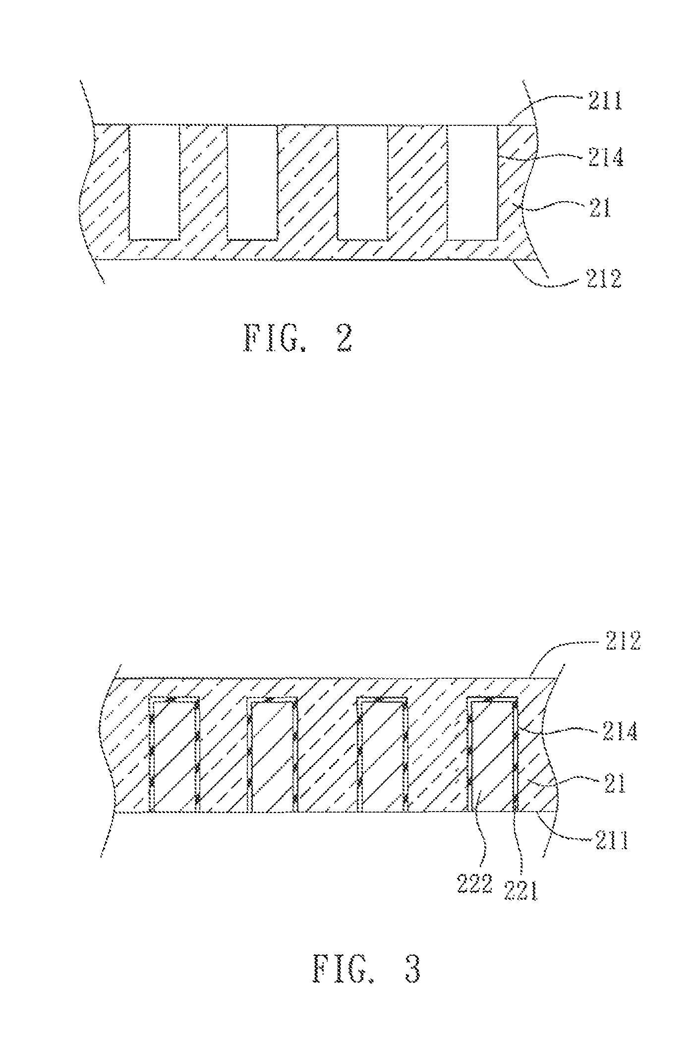
[0018]Referring to FIG. 1A and FIG. 1B, a cross-sectional view and a top view of a semiconductor element having conductive vias according to an embodiment of the present invention are illustrated, respectively. A semiconductor element 20 comprises a silicon substrate 21 and conductive vias 22. The silicon substrate 21 has a first surface 211, a second surface 212 and through holes 213 which penetrate the silicon substrate 21. The thickness (E) of the silicon substrate 21 should be at least about 75 μm, preferably, substantially in a range from 75 to 150 μm.

[0019]The conductive vias 22 are formed within the through holes 213. Each of the conductive vias 22 comprises a first insulation layer 221 and a conductive metal 222, the first insulation layer 221 disposed on a side wall of the through hole 213, defining a first central hole 224. The conductive metal 222 is disposed in the first central hole 224. The first insulation layer 221 can be made of a polymer material with a CTE (Coeffi...


PUM


Abstract

The present invention relates to a semiconductor element having conductive vias and a semiconductor package having a semiconductor element with conductive vias and a method for making the same. The semiconductor element having conductive vias includes a silicon substrate and at least one conductive via. The thickness of the silicon substrate is substantially in a range from 75 to 150 μm. The conductive via includes a first insulation layer and a conductive metal, and the thickness of the first insulation layer is substantially in a range from 5 to 19 μm. Using the semiconductor element and the semiconductor package of the present invention, the electrical connection between the conductive via and the other element can be ensured, and the electrical connection between the silicon substrate and the other semiconductor element can be ensured, so as to raise the yield rate of a product. Moreover, by employing the method of the present invention, warpage and shift of the silicon substrate can be avoided during the reflow process, so as to conduct the reflow process only a single time in the method of the present invention, thereby simplifying the subsequent process and reducing cost.

Description

CROSS-REFERENCE TO RELATED APPLICATIONS[0001]This application claims the benefit of Taiwan application Serial No. 099134620, filed Oct. 11, 2010, the subject matter of which is incorporated herein by reference.BACKGROUND OF THE INVENTION[0002]1. Field of the Invention[0003]The present invention relates to the field of semiconductor packaging, and, more particularly, to the use of conductive vias in semiconductor packages.[0004]2. Description of the Related Art[0005]In recent years, through silicon via (TSV) has become an increasingly popular technique in the field of 3-D semiconductor packaging. In TSV, chips can be stacked on top of one another, and connected using conductive vias which are vertical pathways of interconnects that run through the chips.[0006]Conventionally, a silicon substrate will include a plurality of through holes in which the conductive vias are formed. To avoid placing conductive metal directly on the silicon, each of the conductive vias includes an insulation...

Claims


Application Information

Patent Timeline
Patent Type & Authority Patents(United States)
IPC IPC(8): H01L23/48
CPCH01L2224/05552H01L25/0652H01L2224/92125H01L23/49827H01L2924/01006H01L21/76898H01L2924/3511H01L2224/14181H01L24/81H01L2924/01075H01L24/14H01L2225/06568H01L2924/15311H01L2924/00014H01L2224/81815H01L2225/06565H01L2224/0401H01L24/92H01L25/0655H01L24/06H01L2224/0557H01L23/147H01L2224/73204H01L2924/01033H01L2924/01005H01L2224/05572H01L25/50H01L2924/1432H01L2924/1434H01L24/16H01L24/97H01L2225/06517H01L2924/10253H01L2225/06513H01L2224/16235H01L2225/06541H01L21/563H01L2224/16227H01L2224/06181H01L2924/157H01L2924/01029H01L2224/16225H01L2224/97H01L24/05H01L2224/16146H01L2924/15165H01L24/73H01L25/0657H01L2924/181H01L2224/81H01L2924/00
Inventor WANG, MENG-JEN
Owner ADVANCED SEMICON ENG INC
Why Eureka
Try Eureka