Electro-optical device and electronic apparatus

a technology of optical devices and electronic devices, applied in electrical devices, semiconductor devices, instruments, etc., can solve the problems of ineffective use of capacitance wiring area, inability to completely cover the relay wiring with shield layer, etc., and achieve the effect of improving display quality

Active Publication Date: 2014-09-02
138 EAST LCD ADVANCEMENTS LTD
View PDF10 Cites 235 Cited by
  • Summary
  • Abstract
  • Description
  • Claims
  • Application Information

AI Technical Summary

Benefits of technology

[0009]According to this configuration, since the first capacitance electrode is arranged to be covered with the dielectric layer and the second capacitance electrode, it is possible to increase the area where the first capacitance electrode overlaps with the dielectric layer and the second capacitance electrode compared to a case where the dielectric layer and the second capacitance electrode are merely arranged on the first capacitance electrode such as in the related art. That is, it is possible to increase the area by using a side wall of the first capacitance electrode. As such, it is possible to increase the capacitance of the capacitance element to be greater than the related art. In addition, it is possible to effectively use the area of the capacitance electrodes.Application Example 2
[0011]According to this configuration, since the first insulation film is provided between the pixel electrode connected to the second source and drain electrode and the second capacitance electrode, even if the pixel electrode and the second capacitance electrode are connected through the first contact hole, it is possible to position the second capacitance electrode so as to cover the first capacitance electrode. As such, it is possible to effectively use the area of the capacitance electrode and it is possible to increase the capacitance of the capacitance element without reducing the capacitance area of the capacitance element. Furthermore, it is possible to prevent the position of the first contact hole from being adversely affected.Application Example 3
[0021]According to this configuration, since the electro-optical device described above is provided, it is possible to supply an electronic apparatus which is able to improve display quality.

Problems solved by technology

However, since a relay wiring which is connected to the pixel electrode via a contact hole is arranged in a lower layer than the shield layer, it is not possible for the relay wiring to be completely covered by the shield layer.
In other words, in a case where the relay wiring is used as a capacitance wiring, there is a problem that the area of the capacitance wiring is not able to be effectively used.

Method used


Image

  • Electro-optical device and electronic apparatus
  • Electro-optical device and electronic apparatus
  • Electro-optical device and electronic apparatus

Examples


first embodiment

Configuration of Electro-Optical Device

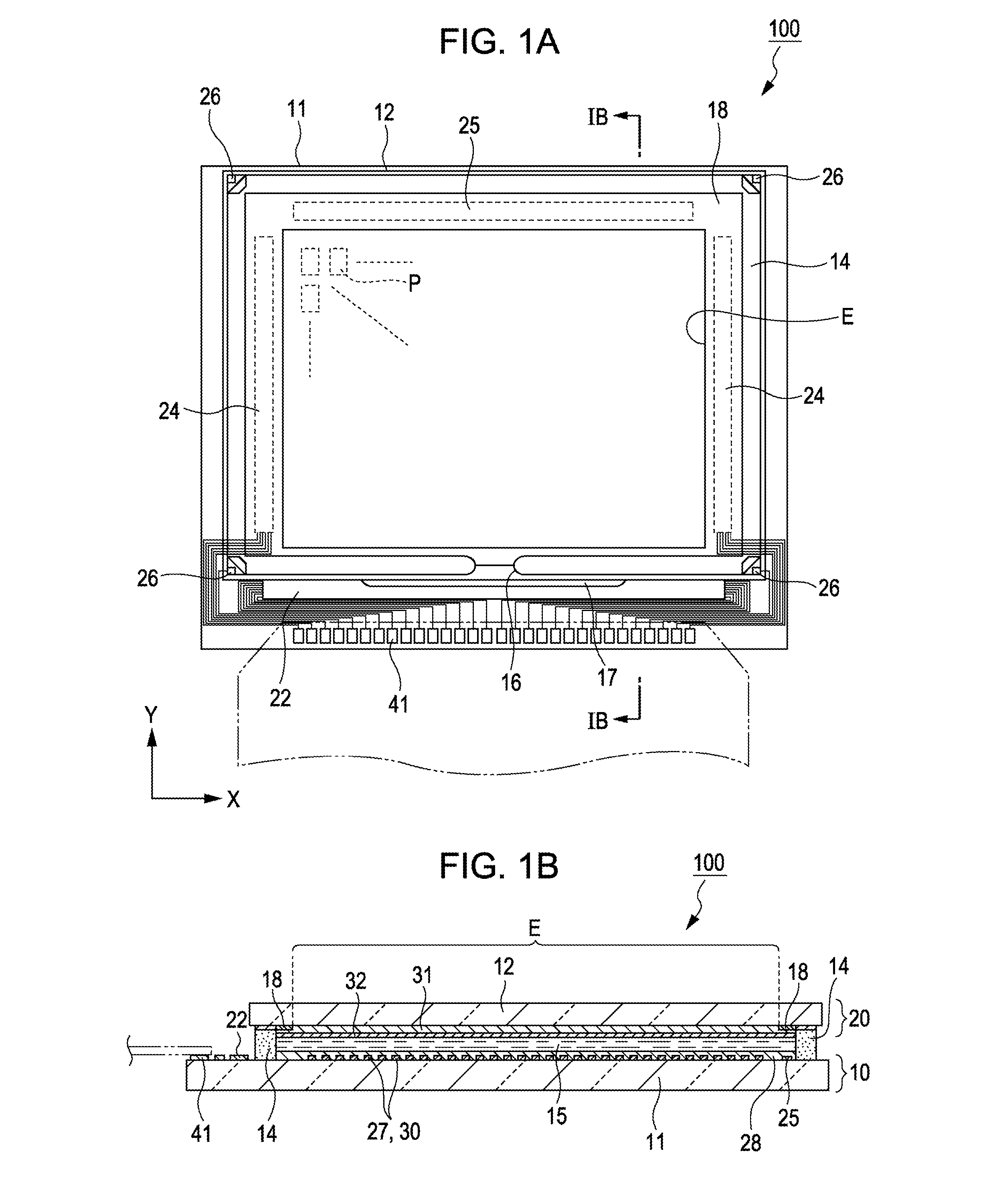
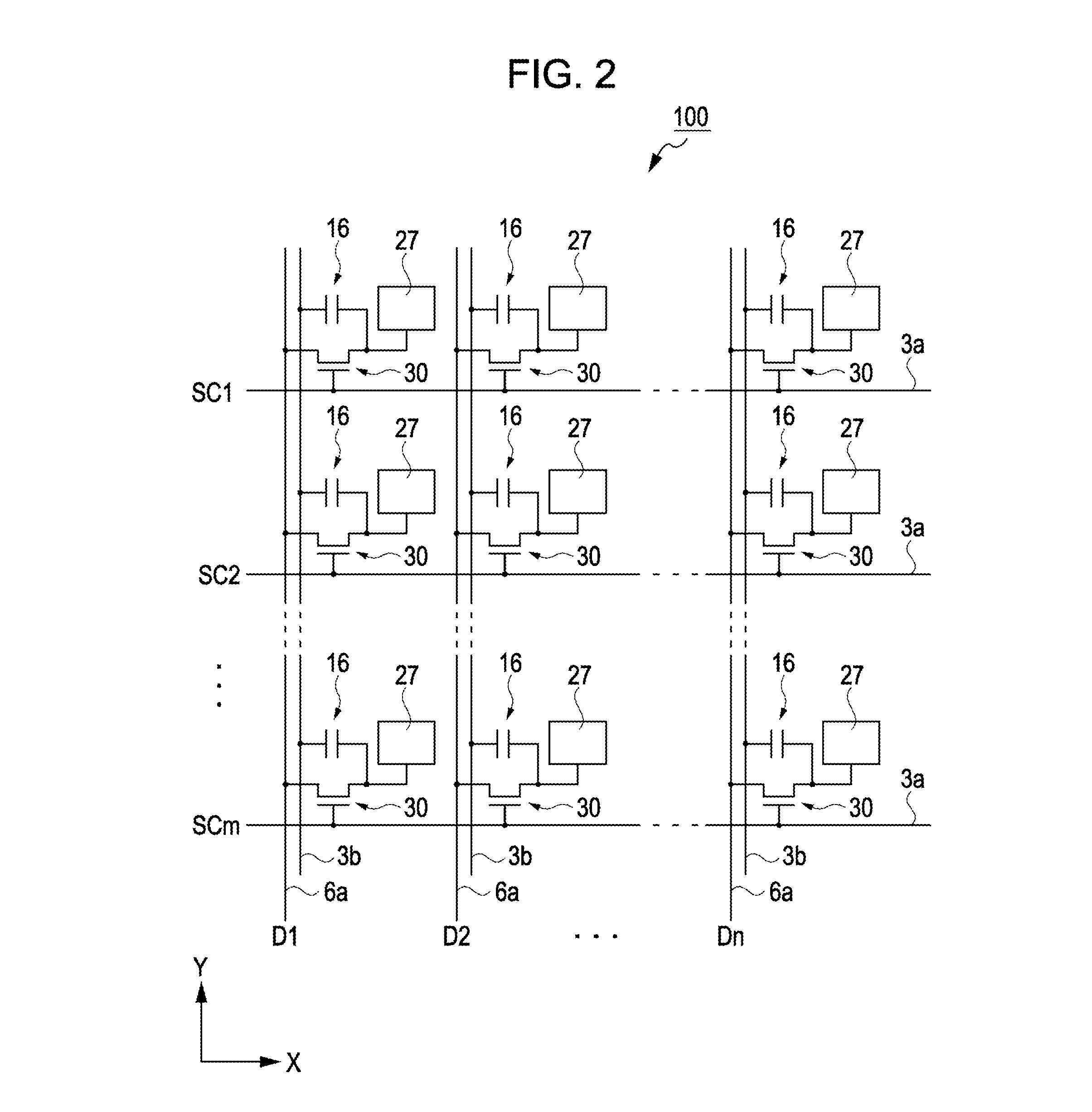
[0036]FIG. 1A is a schematic plan view illustrating a configuration of a liquid crystal device as an electro-optical device. FIG. 1B is a schematic cross-sectional view along a line IB-IB of the liquid crystal device illustrated in FIG. 1A. FIG. 2 is an equivalent circuit view illustrating an electrical configuration of the liquid crystal device. Below, a structure of the liquid crystal device will be described with reference to FIGS. 1A, 1B, and 2.

[0037]As illustrated in FIGS. 1A and 1B, a liquid crystal device 100 of the present embodiment has an element substrate 10 and an opposing substrate 20 which are arranged to oppose, and a liquid crystal layer 15 which is interposed between the pair of substrates. A first substrate 11 which is composed of the element substrate 10 and a second substrate 12 which is composed of the opposing substrate 20 use a transparent glass substrate such as, for example, quartz or the like.

[0038]The element substrat...

second embodiment

Configuration of Electro-Optical Device

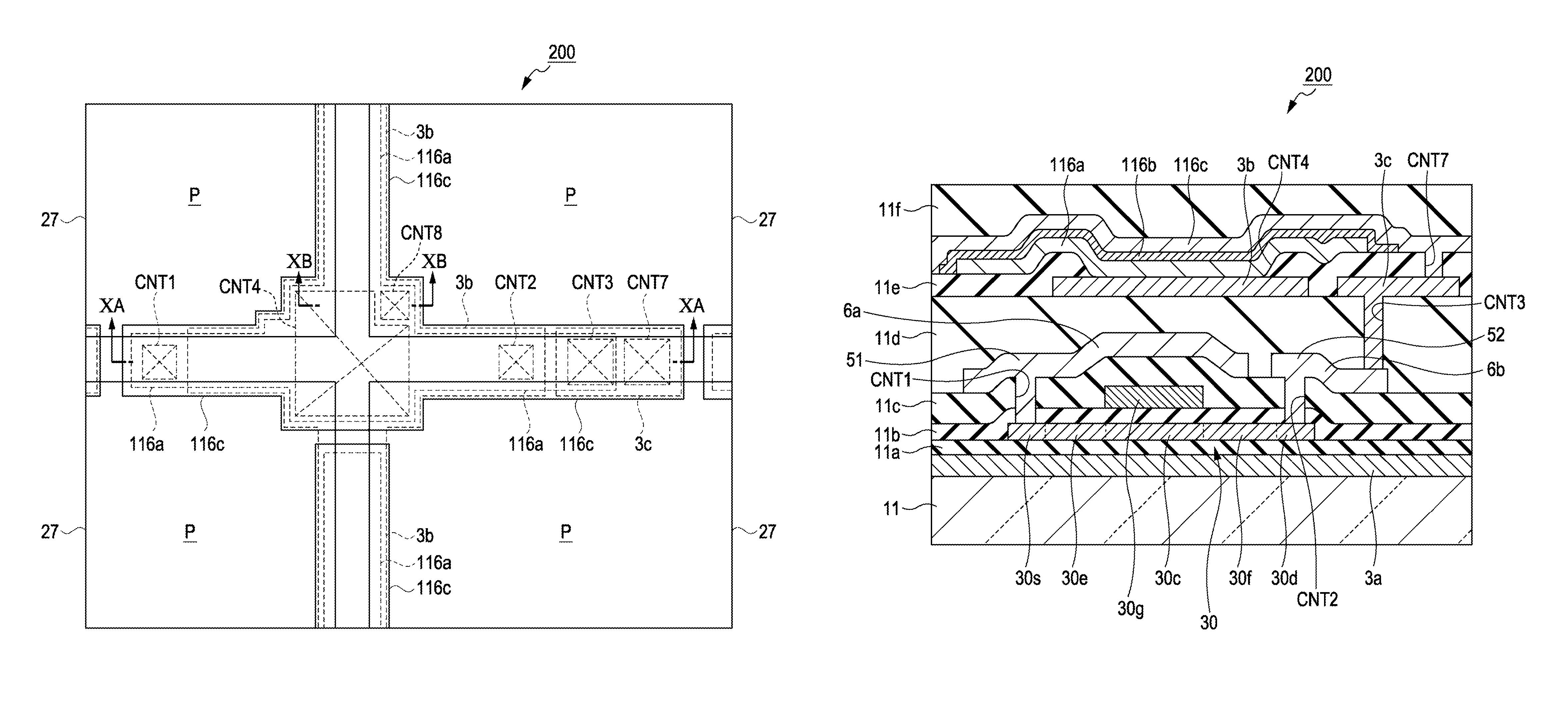
[0119]FIG. 9 is a schematic plan view illustrating a configuration of a liquid crystal device as an electro-optical device according to a second embodiment. FIG. 10 is a schematic cross-sectional view along a line X-X of the liquid crystal device of FIG. 9. Below, a planar structure and a cross-sectional structure of a pixel will be described with reference to FIGS. 9 and 10.

[0120]A liquid crystal device 200 of the second embodiment is different in the structure of the capacitance element 116 and is generally the same in the other configurations compared to the first embodiment described above. For this reason, in the second embodiment, differences with the first embodiment will be described while other same description thereof will be omitted.

[0121]As shown in FIGS. 9 and 10, in the liquid crystal device 200 of the second embodiment, the capacitance line 3b is provided to overlap with a portion of the data line 6a and a portion of the scanning...

modification example 1

[0131]As described above, two capacitance electrodes 16a and 16c which configure the capacitance element 16 is not limited to being configured by a metal layer (aluminum, titanium nitride, and the like) and may be configured by, for example, a transparent conductive film such as ITO.


PUM

PropertyMeasurementUnit
thicknessaaaaaaaaaa
thicknessaaaaaaaaaa
thicknessaaaaaaaaaa

Abstract

Disclosed is a pixel electrode which is electrically connected to a scanning line electrically connected to a gate electrode, a data line electrically connected to a data line side source and drain region, and a pixel electrode side source and drain region; and a capacitance element which has a first capacitance electrode which is electrically connected to a capacitance line, a second capacitance electrode which is provided to oppose the first capacitance electrode, and a dielectric layer which is interposed between the first capacitance electrode and the second capacitance electrode, where the first capacitance electrode is arranged to be covered with the dielectric layer and the second capacitance electrode between a layer where the transistor, the scanning line, and the data line are provided and a layer where the pixel electrode is provided.

Description

BACKGROUND[0001]1. Technical Field[0002]The present invention relates to an electro-optical device and an electronic apparatus.[0003]2. Related Art[0004]As the electro-optical device, an active driven type liquid crystal device, where a switching element such as a thin film transistor is provided for each pixel, is known. The active driven type liquid crystal device has a liquid crystal layer between a pair of electrodes, and an image signal written into each pixel is temporarily held in an electric capacitance consisting of the pair of electrodes and the liquid crystal layer. In addition to this, a capacitance element, which electrically holds the image signal for a predetermined period, is provided for each pixel.[0005]For example, in JP-A-2010-39212, providing a capacitance element by overlapping the position of relay wiring connected to a pixel electrode with a shield layer via a dielectric layer on the upper layer thereof is disclosed.[0006]However, since a relay wiring which i...

Claims


Application Information

Patent Timeline
Patent Type & Authority Patents(United States)
IPC IPC(8): H01L27/06G02F1/1362H01L27/12
CPCH01L27/1255G02F1/136286G02F1/136213G02F2201/40
Inventor OYAMADA, SHIN
Owner 138 EAST LCD ADVANCEMENTS LTD
Why Eureka
Try Eureka