Method for heating part in processing chamber of semiconductor manufacturing apparatus and semiconductor manufacturing apparatus

a technology of semiconductor manufacturing apparatus and processing chamber, which is applied in lighting and heating apparatus, household stoves or ranges, stoves, etc., can solve the problems of high frequency power leakage from wiring, redesign of apparatus, and increase manufacturing costs, and achieves simple and easy configuration and efficient heating of parts.

Active Publication Date: 2014-09-02
TOKYO ELECTRON LTD
View PDF11 Cites 3 Cited by
  • Summary
  • Abstract
  • Description
  • Claims
  • Application Information

AI Technical Summary

Benefits of technology

[0008]In view of the foregoing, the present disclosure provides a method for heating a part in a processing chamber of a semiconductor manufacturing apparatus having a simple and easy configuration capable of efficiently heating the part in the processing chamber and also provides a semiconductor manufacturing apparatus.
[0011]In accordance with the present disclosure, it is possible to provide a method for heating a part in a processing chamber of a semiconductor manufacturing apparatus having a simple and easy configuration capable of efficiently heating the part in the processing chamber and a semiconductor manufacturing apparatus.

Problems solved by technology

However, by way of example, in a semiconductor manufacturing apparatus which generates plasma by a high frequency power in a processing chamber, an abnormal electric discharge may be generated toward a wiring for supplying electric power to a heater of a focus ring and the high frequency power may leak from the wiring.
Thus, it may be required to redesign the apparatus and manufacturing costs may increase.

Method used


Image

  • Method for heating part in processing chamber of semiconductor manufacturing apparatus and semiconductor manufacturing apparatus
  • Method for heating part in processing chamber of semiconductor manufacturing apparatus and semiconductor manufacturing apparatus
  • Method for heating part in processing chamber of semiconductor manufacturing apparatus and semiconductor manufacturing apparatus

Examples


Embodiment Construction

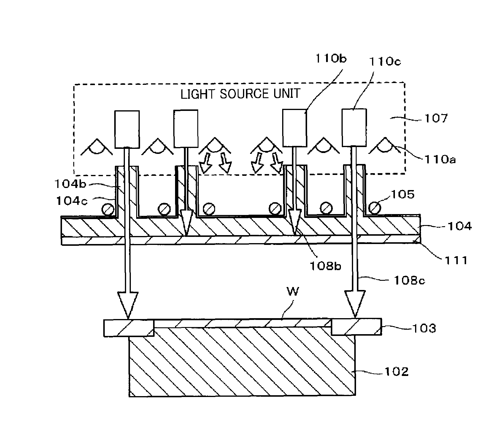
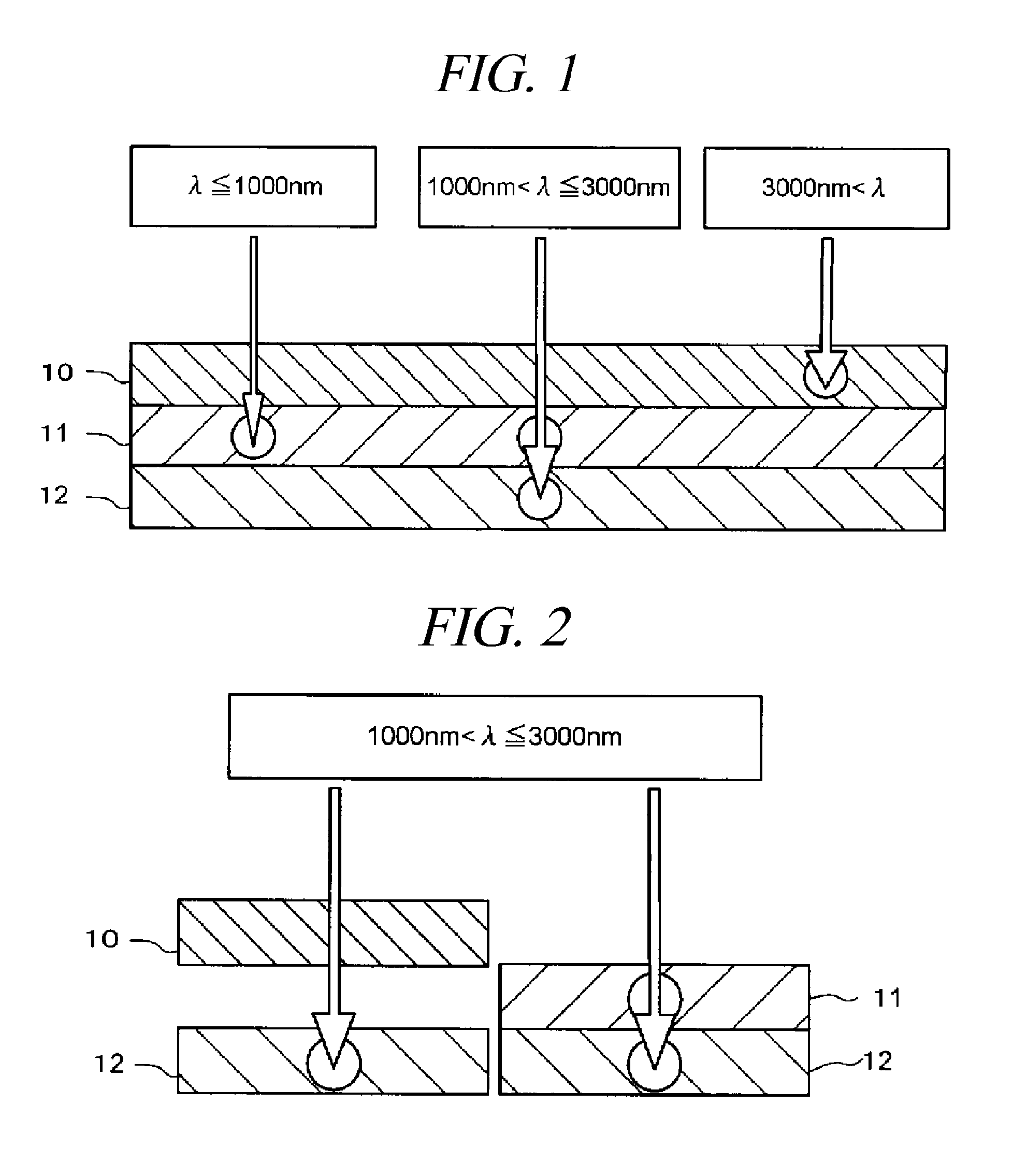
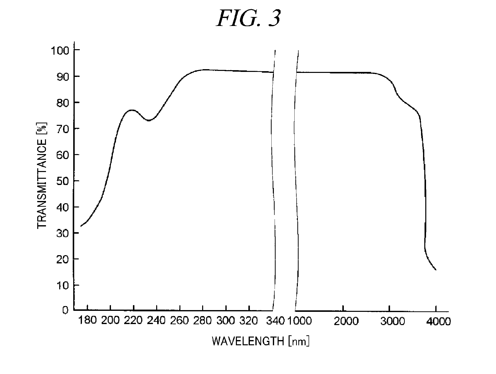
[0023]Hereinafter, embodiments of the present disclosure will be described in detail with reference to the accompanying drawings. FIG. 1 is a view for explaining a method for heating a part in a processing chamber of a semiconductor manufacturing apparatus in accordance with the present embodiment.

[0024]In an example illustrated in FIG. 1, as parts within the processing chamber of the semiconductor manufacturing apparatus, a part 10 made of quartz is provided at an uppermost position of a processing chamber; a part 11 made of silicon is provided under the quartz part 10; and a part 12 made of ceramic such as alumina is provided under the silicon part 11. It may be possible to use a part made of silicon carbide (SiC) or carbon (C) in the processing chamber instead of using the silicon part 11 in the processing chamber. It may be possible to use a part coated with a diamond-like carbon film in the processing chamber instead of using the silicon part 11 in the processing chamber and it...


PUM

PropertyMeasurementUnit
wavelength bandaaaaaaaaaa
thicknessaaaaaaaaaa

Abstract

There is provided a method for heating a part within a processing chamber of a semiconductor manufacturing apparatus having a substrate in the processing chamber and performing a process on the substrate. The heating method includes generating heating lights which is generated by a heating light source provided outside the processing chamber and has a wavelength band capable of passing through a first part in the processing chamber and being absorbed into a second part in the processing chamber made of a material different from that of the first part, and heating the second part in the processing chamber by passing the heating lights through the first part in the processing chamber and irradiating the heating lights to the second part in the processing chamber.

Description

CROSS-REFERENCE TO RELATED APPLICATION[0001]This application claims the benefit of Japanese Patent Application No. 2010-042036 filed on Feb. 26, 2010 and U.S. Provisional Application Ser. No. 61 / 282,660 filed on Mar. 15, 2010, the entire disclosures of which are incorporated herein by reference.FIELD OF THE INVENTION[0002]The present disclosure relates to a method for heating a part in a processing chamber of a semiconductor manufacturing apparatus such as a plasma processing apparatus and also relates to a semiconductor manufacturing apparatus.BACKGROUND OF THE INVENTION[0003]Conventionally, in a semiconductor device manufacturing process performed by a semiconductor manufacturing apparatus, a substrate such as a semiconductor wafer or a glass substrate for liquid crystal display has been accommodated in an airtightly sealed processing chamber and an etching process or a film forming process has been performed by plasma or the like in the processing chamber.[0004]Further, by way of...

Claims


Application Information

Patent Timeline
Patent Type & Authority Patents(United States)
IPC IPC(8): A21B2/00F26B19/00
CPCH01L21/67115F27B17/0025F27D11/12H01L21/02H01L21/02266H01L21/203H01L21/205H01L21/302H01L21/3065H01L21/31116H01L21/324H01L21/67098H01L21/76825H01L21/76826H05H1/46
Inventor YAMAWAKU, JUNKOSHIMIZU, CHISHIOMATSUDO, TATSUO
Owner TOKYO ELECTRON LTD
Why Eureka
Try Eureka