ReRAM stacks preparation by using single ALD or PVD chamber

a technology of reram and stack, which is applied in the direction of coating, chemical vapor deposition coating, instruments, etc., can solve the problems of increased throughput and decreased cost, and achieve the effects of reducing device exposure to air and particulates, increasing throughput and cos

Inactive Publication Date: 2014-09-30
SANDISK TECH LLC +2
View PDF37 Cites 34 Cited by
  • Summary
  • Abstract
  • Description
  • Claims
  • Application Information

AI Technical Summary

Benefits of technology

[0010]Systems and methods for preparing resistive switching memory devices such as resistive random access memory (ReRAM) devices wherein both oxide and nitride layers are deposited in a single tool are provided. In some embodiments, a single tool is comprised of one or more atomic layer deposition (ALD) or chemical vapor deposition (CVD) chambers and one or more physical vapor deposition (PVD) chambers coupled together by a transfer chamber. Various oxide and nitride based layers in the ReRAM device such as the switching layer, current-limiting layer, and the top electrode (and optionally the bottom electrode) are deposited in the single tool. By fabricating the ReRAM device in a single tool having multiple chambers, throughput is increased and cost is decreased. Moreover, processing in a single tool reduces device exposure to air and to particulates, thereby minimizing device defects.

Problems solved by technology

By fabricating the ReRAM device in a single tool having multiple chambers, throughput is increased and cost is decreased.

Method used


Image

  • ReRAM stacks preparation by using single ALD or PVD chamber
  • ReRAM stacks preparation by using single ALD or PVD chamber
  • ReRAM stacks preparation by using single ALD or PVD chamber

Examples


example 1

Single Chamber

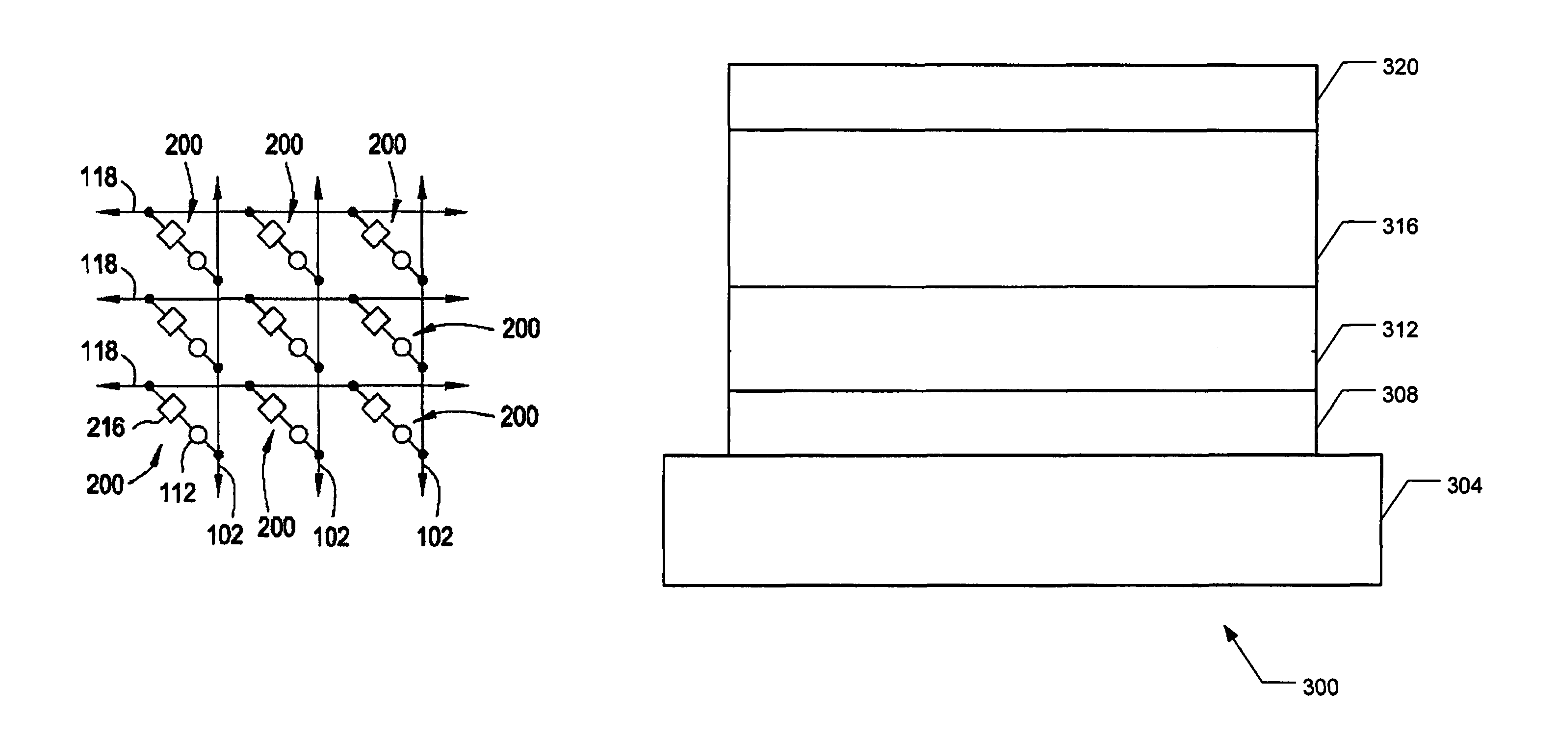
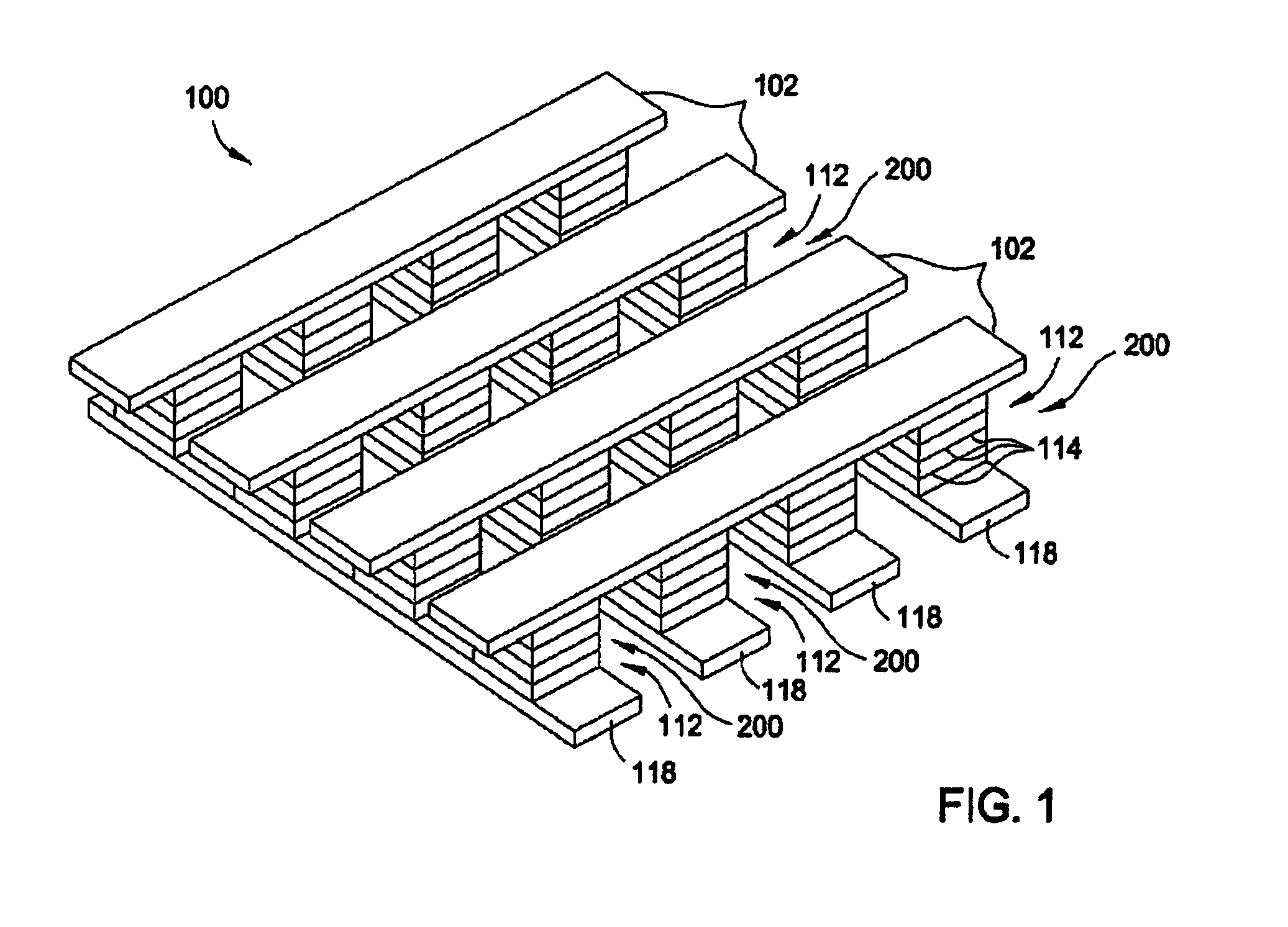
[0059]Place a substrate into chamber 1 and deposit switching layer (312) on the wafer according to the following ALD deposition conditions: Substrate temperature fixed between 200-350 C, chamber pressure between 0.5-2.0 Torr, repeat ALD cycles to form a layer of desired thickness: using approximately 100-500 sccm Ar carrier gas to deliver the metal precursor (i.e. one of TDMAHf, TEMAHf, HfCl4, TDMATi, TEMATi, TiCl4, TMA, TEMAZr, ZyALD™, PDMATa) between 0.5-30 sec, purge ˜200-5000 sccm Ar between 5-60 sec, pulse oxidant (i.e. one of H2O, O3, plasma O2) between 0.5-30 sec, purge approximately ˜200-5000 sccm Ar between 5-60 sec.

[0060]The substrate stays in chamber 1, and the process can continue after purge steps to deposit the current limiting layer (316) according to the following ALD deposition conditions: Substrate temperature fixed between 200-350 C, chamber pressure between 0.5-2.0 Torr, repeat ALD cycles to form a layer of desired thickness: use ˜100-500 sccm Ar ca...

example 2

Single Tool with Multiple Chambers

[0062]Place substrate into chamber 1 and deposit switching layer (312) on the substrate according to the following ALD deposition conditions: Substrate temperature fixed between 200-350 C, chamber pressure between 0.5-2.0 Torr, repeat ALD cycles to form a layer of desired thickness: using approximately 100-500 sccm Ar carrier gas to deliver the metal precursor (i.e. one of TDMAHf, TEMAHf, HfCl4, TDMATi, TEMATi, TiCl4, TMA, TEMAZr, ZyALD™, PDMATa) between 0.5-30 sec, purge approximately 200-5000 sccm Ar between 5-60 sec, pulse oxidant (i.e. one of H2O, O3, plasma O2) between 0.5-30 sec, purge approximately 200-5000 sccm Ar between 5-60 sec.

[0063]The substrate stays in chamber 1 (or may be transferred to another chamber), and the process can continue after purge steps to deposit the current limiting layer (312) according to the following ALD deposition conditions: Substrate temperature fixed between 200-350 C, chamber pressure between 0.5-2.0 Torr, re...


PUM

PropertyMeasurementUnit
temperatureaaaaaaaaaa
voltageaaaaaaaaaa

Abstract

Systems and methods for preparing resistive switching memory devices such as resistive random access memory (ReRAM) devices wherein both oxide and nitride layers are deposited in a single chamber are provided. Various oxide and nitride based layers in the ReRAM device such as the switching layer, current-limiting layer, and the top electrode (and optionally the bottom electrode) are deposited in the single chamber. By fabricating the ReRAM device in a single chamber, throughput is increased and cost is decreased. Moreover, processing in a single chamber reduces device exposure to air and to particulates, thereby minimizing device defects.

Description

TECHNICAL FIELD[0001]The present disclosure relates generally to fabrication of nonvolatile memory elements and in particular to systems and methods for preparing resistive switching memory devices in a single tool.BACKGROUND[0002]Nonvolatile memory elements are used in systems in which persistent storage is required. For example, digital cameras use nonvolatile memory cards to store images and digital music players use nonvolatile memory to store audio data. Nonvolatile memory is also used to persistently store data in computer environments.[0003]Nonvolatile memory is often formed using electrically-erasable programmable read only memory (EEPROM) technology. This type of nonvolatile memory contains floating gate transistors that can be selectively programmed or erased by application of suitable voltages to their terminals.[0004]As fabrication techniques improve, it is becoming possible to fabricate nonvolatile memory elements with increasingly smaller dimensions. However, as device...

Claims


Application Information

Patent Timeline
Patent Type & Authority Patents(United States)
IPC IPC(8): H01L45/00H01L21/20
CPCH01L45/08H01L27/2409H01L27/2463H01L45/12H01L45/1233H01L45/146H01L45/1616H10B63/20H10B63/80H10N70/801H10N70/24H10N70/826H10N70/8833H10N70/023
Inventor LEE, ALBERT SANGHYUPHSUEH, CHIEN-LANMINVIELLE, TIMYAMAGUCHI, TAKESHI
Owner SANDISK TECH LLC
Why Eureka
Try Eureka