Embedded chip-on-chip package and package-on-package comprising same

a chip-on-chip and chip technology, applied in the direction of printed circuit aspects, printed circuit non-printed electric components association, non-metallic protective coating application, etc., can solve the problem that the improvement of wafer manufacturing process is more expensive than the improvement of packaging technique, and achieve the effect of improving internal connections and reducing siz

Active Publication Date: 2014-10-28
SAMSUNG ELECTRONICS CO LTD
View PDF15 Cites 9 Cited by
  • Summary
  • Abstract
  • Description
  • Claims
  • Application Information

AI Technical Summary

Benefits of technology

[0009]These and other embodiments of the inventive concept can provide COC packages and POPs with reduced size and improved internal connections.

Problems solved by technology

In general, improvements in wafer manufacturing processes tend to be more expensive than improvements in packaging techniques.

Method used


Image

  • Embedded chip-on-chip package and package-on-package comprising same
  • Embedded chip-on-chip package and package-on-package comprising same
  • Embedded chip-on-chip package and package-on-package comprising same

Examples


Embodiment Construction

[0016]Embodiments of the inventive concept are described below with reference to the attached drawings. These embodiments are presented as teaching examples and should not be construed to limit the scope of the inventive concept.

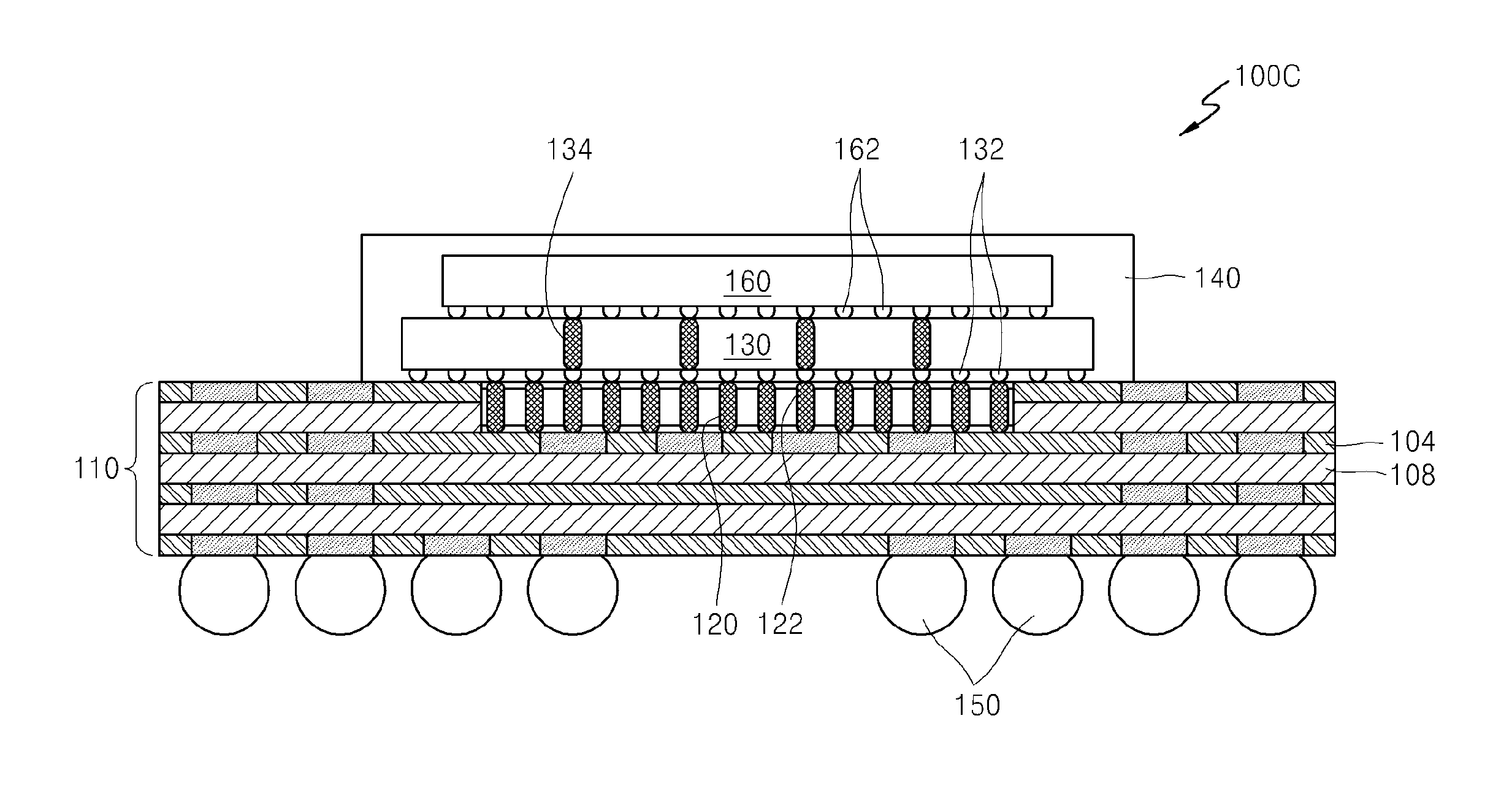
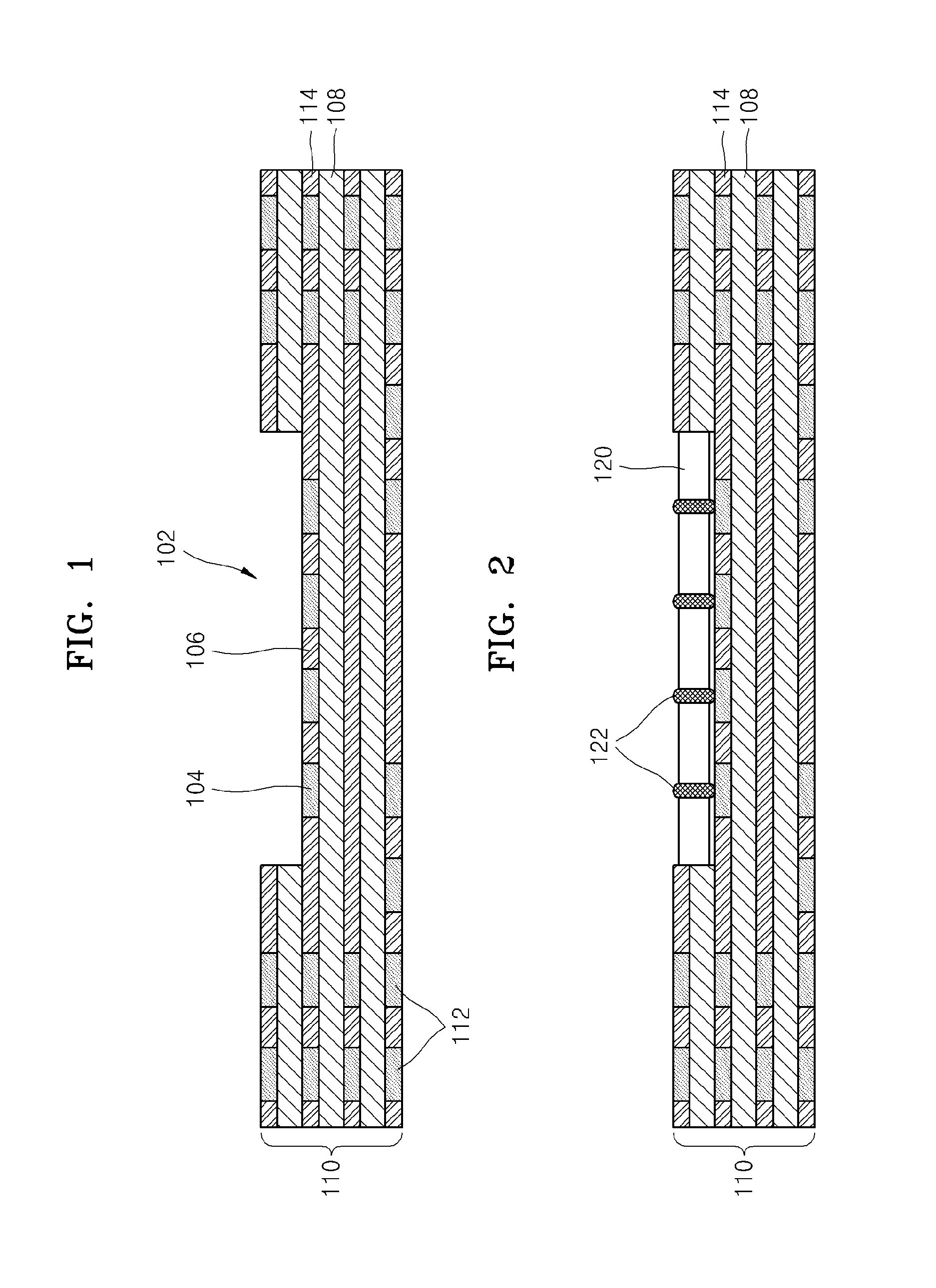
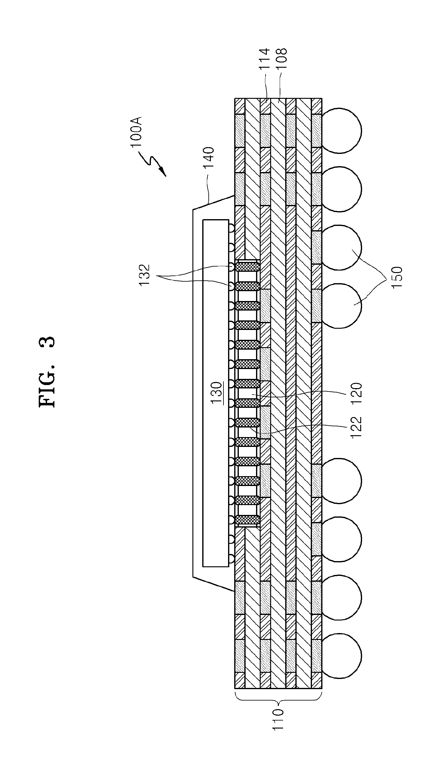
[0017]FIGS. 1 through 3 are cross-sectional views illustrating a method of manufacturing an embedded COC package 100A according to an embodiment of the inventive concept.

[0018]Referring to FIG. 1, a PCB 110 having a multilayer substrate structure is prepared. PCB 110 comprises insulating layers 108 alternately formed with layers 114 having printed circuit patterns 104. PCB 110 comprises a recessed semiconductor chip mounting unit 102 configured to receive a semiconductor chip. Printed circuit patterns 104 and an insulating material 106 that are connectable to pads of the semiconductor chip are formed on a bottom surface of recessed semiconductor chip mounting unit 102.

[0019]In some embodiments, PCB 110 comprises bond fingers (not shown) on an upper surface a...


PUM


Abstract

An embedded chip-on-chip package includes a printed circuit board having a recessed semiconductor chip mounting unit constituted by a recess in the printed circuit board and a circuit pattern at the bottom of the recess, a first semiconductor chip embedded in the recessed semiconductor chip mounting unit and electrically connected to the circuit pattern at the bottom of the recess, and a second semiconductor chip mounted to the recessed semiconductor chip mounting unit and electrically connected to the first semiconductor chip and the printed circuit board independently of each other.

Description

CROSS-REFERENCE TO RELATED APPLICATIONS[0001]This application claims priority under 35 U.S.C. §119 to Korean Patent Application No. 10-2010-0062080 filed on Jun. 29, 2010, the disclosure of which is hereby incorporated by reference in its entirety.BACKGROUND OF THE INVENTION[0002]Embodiments of the inventive concept relate generally to integrated circuit packaging. More particularly, embodiments of the inventive concept relate to a chip-on-chip (COC) semiconductor package comprising one or more semiconductor chips, and a package-on-package (POP) incorporating the COC semiconductor package.[0003]In response to increasing demand for electronic data processing capability, researchers are continually striving to improve the performance and functionality of semiconductor devices. One way to increase performance is by increasing the integration density of the devices through improved wafer manufacturing processes. Another way to increase performance is by reducing the footprint of the dev...

Claims


Application Information

Patent Timeline
Patent Type & Authority Patents(United States)
IPC IPC(8): H05K3/28H05K1/18H05K3/34H01L25/065H01L25/10
CPCH01L2224/16225H01L25/105H01L2924/15153H01L2225/1058H01L2225/1023H01L2224/16145H01L2224/32225H01L2224/48227H05K2201/10515H01L2924/15311H05K3/284H01L2224/73265H01L2225/06541H05K1/183H05K2201/1053H01L2224/16227H01L2225/06565H01L2924/15331H01L25/0657H05K3/3436H01L24/73H01L2924/14H01L2924/00014H01L2224/13025H01L2224/16146H01L2224/17181H01L2924/00012H01L2924/00H01L2224/0401
Inventor KIM, YONG-HOONLEE, HEE-SEOK
Owner SAMSUNG ELECTRONICS CO LTD
Why Eureka
Try Eureka