Semiconductor device and method for manufacturing semiconductor device

a semiconductor and semiconductor technology, applied in the direction of semiconductor devices, basic electric elements, electrical equipment, etc., can solve the problems of reducing the yield of transistors in the manufacturing process, and achieve the effects of high integration, low power consumption, and high speed operation

Inactive Publication Date: 2014-11-04
SEMICON ENERGY LAB CO LTD
View PDF135 Cites 6 Cited by
  • Summary
  • Abstract
  • Description
  • Claims
  • Application Information

AI Technical Summary

Benefits of technology

[0009]In order to achieve high-speed operation, low power consumption, high integration, or the like of a transistor, it is necessary to miniaturize a transistor.
[0010]It is desirable to improve the on-state characteristics (e.g., on-state current and field-effect mobility) of the miniaturized transistor for high-speed response and high-speed driving of a semiconductor device. To suppress a decrease in on-state current of a transistor, it is effective to provide a gate electrode layer in a region (hereinafter, also referred to as a Lov region in this specification) where the gate electrode layer overlaps with a source electrode layer or a drain electrode layer with a gate insulating layer provided therebetween.
[0011]However, precise alignment between an oxide semiconductor layer with a narrow line width and a gate electrode layer with a narrow line width is required for formation of an Lov region, and the required accuracy thereof is increased in accordance with miniaturization of the transistor. Accordingly, it is concerned that yield of transistors in the manufacturing process is decreased due to miniaturization thereof.

Problems solved by technology

Accordingly, it is concerned that yield of transistors in the manufacturing process is decreased due to miniaturization thereof.

Method used


Image

  • Semiconductor device and method for manufacturing semiconductor device
  • Semiconductor device and method for manufacturing semiconductor device
  • Semiconductor device and method for manufacturing semiconductor device

Examples


embodiment 1

(Embodiment 1)

[0048]In this embodiment, an embodiment of a semiconductor device and a method for manufacturing the semiconductor device are described with reference to FIGS. 1A and 1B, FIGS. 2A and 2B, FIGS. 3A to 3D, and FIGS. 4A to 4D.

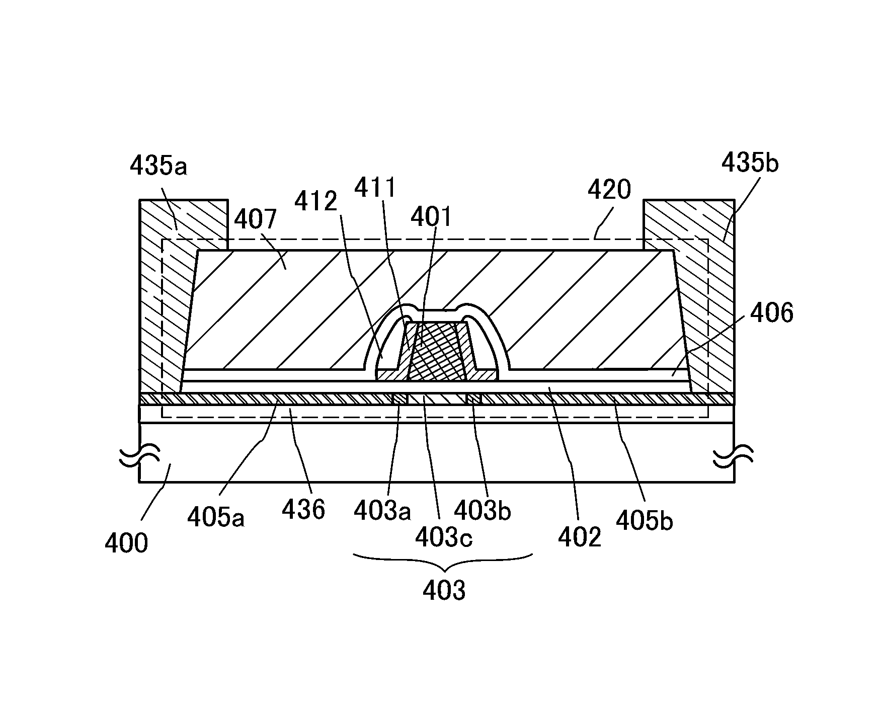
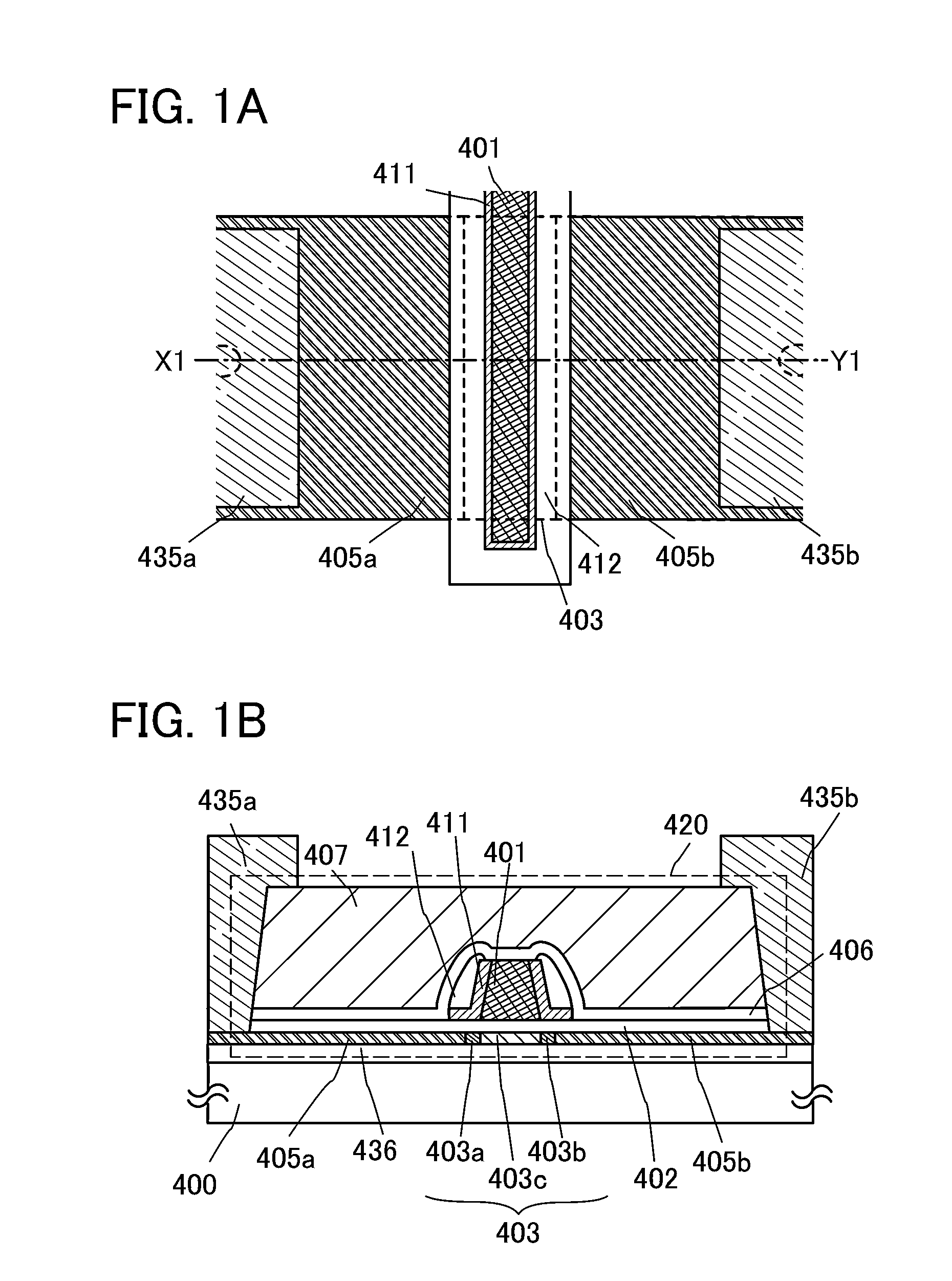
[0049]As an example of a semiconductor device, a plan view and a cross-sectional view of a transistor 420 are illustrated in FIGS. 1A and 1B, respectively. FIG. 1A is a plan view of the transistor 420, and FIG. 1B is a cross-sectional view taken along the line X1-Y1 in FIG. 1A. Note that in FIG. 1A, some components of the transistor 420 (e.g., an insulating layer 407 and the like) are not illustrated for simplicity.

[0050]The transistor 420 illustrated in FIGS. 1A and 1B includes, over a substrate 400 having an insulation surface, a base insulating layer 436; a source electrode layer 405a and a drain electrode layer 405b; an oxide semiconductor layer 403 including an impurity region 403a, an impurity region 403b, and a channel formation region 403c; a...

embodiment 2

(Embodiment 2)

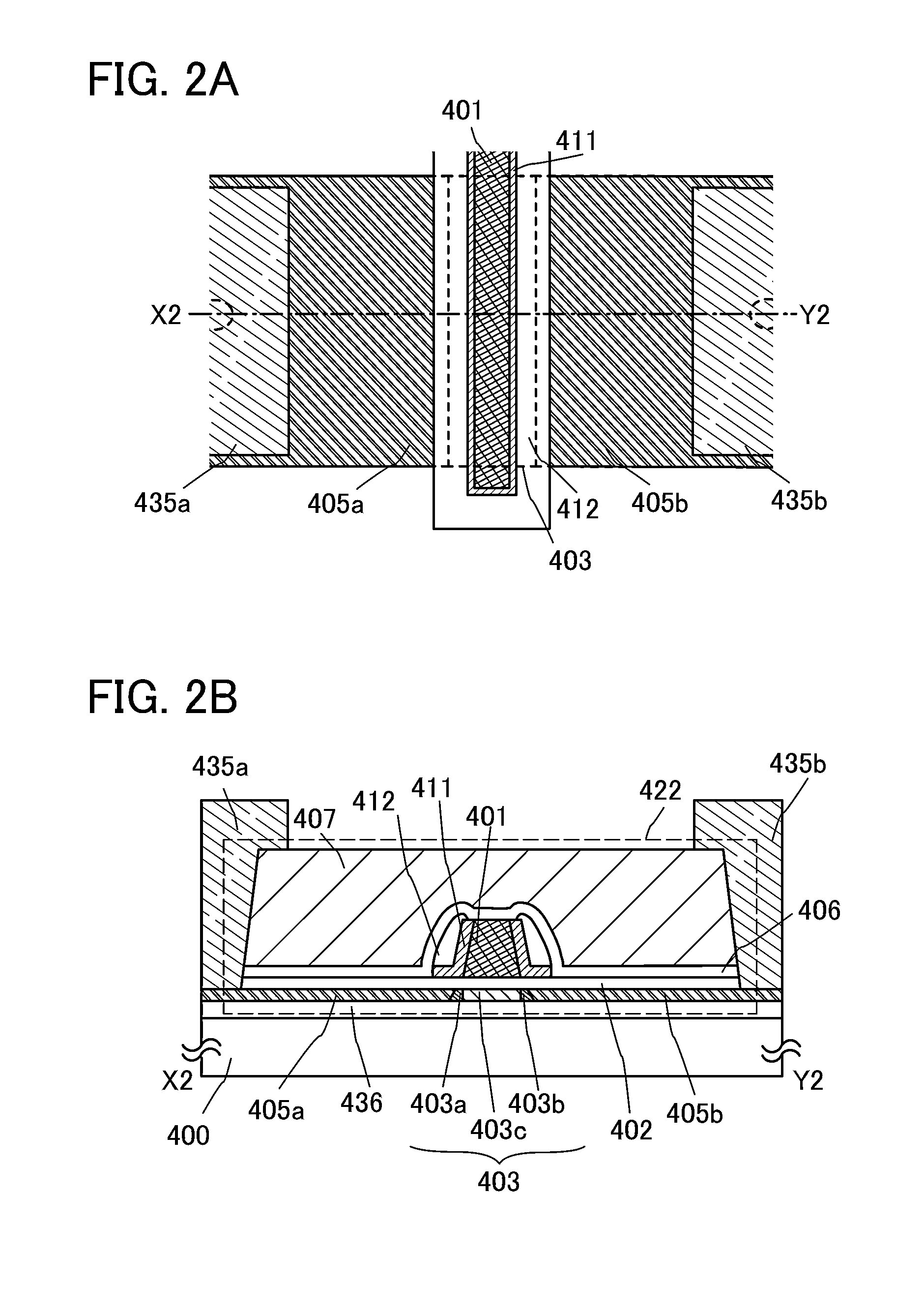
[0164]In this embodiment, a structure and a manufacturing method of a semiconductor device according to an embodiment of the disclosed invention, which are different from those of Embodiment 1, will be described with reference to FIGS. 5A and 5B, FIGS. 6A to 6D, and FIGS. 7A to 7C. The same portions as those in Embodiment 1 and portions having functions similar to those in Embodiment 1 and the same steps as those in Embodiment 1 and steps similar to those in Embodiment 1 can be conducted as in Embodiment 1, and repeated description is skipped. In addition, detailed description of the same portion is skipped.

[0165]FIGS. 5A and 5B are respectively a plan view and a cross-sectional view which illustrate a transistor 424 as another example of a semiconductor device. FIG. 5A is a plan view of the transistor 424, and FIG. 5B is a cross-sectional view taken along line X3-Y3 in FIG. 5A. Note that in FIG. 5A, some components of the transistor 424 (e.g., an insulating layer 407)...

embodiment 3

(Embodiment 3)

[0189]In this embodiment, an example of a semiconductor device which includes the transistor described in this specification, which can hold stored data even when not powered, and which does not have a limitation on the number of write cycles, will be described with reference to drawings.

[0190]FIGS. 8A and 8B illustrate an example of a structure of a semiconductor device. FIG. 8A is a cross-sectional diagram of the semiconductor device, FIG. 8B is a plan view of the semiconductor device, and FIG. 8C is a circuit diagram of the semiconductor device. Here, FIG. 8A corresponds to a cross section along line C1-C2 and line D1-D2 in FIG. 8B.

[0191]The semiconductor device illustrated in FIGS. 8A and 8B includes a transistor 160 using a first semiconductor material in its lower portion, and a transistor 162 using a second semiconductor material in its upper portion. The transistor of an embodiment of the present invention described in Embodiment 1 or 2 can be employed as the t...


PUM


Abstract

Provided is a miniaturized transistor having high electrical characteristics. The transistor includes a source electrode layer in contact with one side surface of the oxide semiconductor layer in the channel-length direction and a drain electrode layer in contact with the other side surface thereof. The transistor further includes a gate electrode layer in a region overlapping with a channel formation region with a gate insulating layer provided therebetween and a conductive layer having a function as part of the gate electrode layer in a region overlapping with the source electrode layer or the drain electrode layer with the gate insulating layer provided therebetween and in contact with a side surface of the gate electrode layer. With such a structure, an Lov region is formed with a scaled-down channel length maintained.

Description

BACKGROUND OF THE INVENTION[0001]1. Field of the Invention[0002]The present invention relates to a semiconductor device and a method for manufacturing the semiconductor device.[0003]In this specification and the like, a semiconductor device refers to all types of devices which can function by utilizing semiconductor characteristics; an electro-optical device, a light-emitting display device, a semiconductor circuit, and an electronic device are all semiconductor devices.[0004]2. Description of the Related Art[0005]A technique by which transistors are formed using semiconductor thin films formed over a substrate having an insulation surface has been attracting attention. The transistor is applied to a wide range of semiconductor devices such as an integrated circuit (IC) and an image display device (also simply referred to as display device). A silicon-based semiconductor material is widely known as a material for a semiconductor thin film applicable to a transistor. As another mater...

Claims


Application Information

Patent Timeline
Patent Type & Authority Patents(United States)
IPC IPC(8): H01L29/78H01L21/34H01L29/12
CPCH01L21/02581H01L21/02565H01L29/78618H01L29/4908H01L29/42384H01L27/1225H01L21/02554H01L21/02631H01L29/66969H01L29/7869H01L29/78H01L21/34H01L29/41733H01L29/66742
Inventor SASAGAWA, SHINYAKURATA, MOTOMU
Owner SEMICON ENERGY LAB CO LTD
Why Eureka
Try Eureka