Method for measuring and controlling distance between lower end surface of heat shielding member and surface of raw material melt and method for manufacturing silicon single crystal

a technology of heat shielding member and lower end surface, which is applied in the direction of crystal growth process, instruments, and under a protective fluid, can solve the problems of difficult to precisely control the dpm, increase the effect of defects, and increase the problem of grown-in defects in silicon wafers, etc., and achieves high quality, high precision, and measurement more stably and precisely

Active Publication Date: 2014-11-11
SHIN-ETSU HANDOTAI CO LTD
View PDF15 Cites 0 Cited by
  • Summary
  • Abstract
  • Description
  • Claims
  • Application Information

AI Technical Summary

Benefits of technology

[0040]As described above, according to the method for measuring a distance between a lower end surface of a heat shielding member and a surface of a raw material melt of the present invention, the distance between the lower end surface of the heat shielding member and the surface of the raw material melt can be measured more stably and precisely. Controlling the distance between the lower end surface of the heat shielding member and the surface of the raw material melt on the basis of the measurement result enables highly precise control of the distance between the lower end surface of the heat shielding member and the surface of the raw material melt. Therefore, the crystal axis temperature gradient in the direction of the crystal growth axis can be controlled highly precisely, and a high quality silicon single crystal can be efficiently manufactured at high productivity. In addition, when the distance between the lower end surface of the heat shielding member and the surface of the raw material melt is controlled such that it is more than the lowest limit, the contact between the lower end surface of the heat shielding member and the surface of the raw material melt can be prevented, and the silicon single crystal can be grown safely.

Problems solved by technology

In recent years, grown-in defects in silicon wafers becomes an issue as higher integration of semiconductor devices and accompanying shrinking feature sizes are advanced.
The grown-in defect is a factor in deteriorated characteristics of semiconductor devices and the advancement of the shrinking feature sizes of a device is heightening the effect of the defect.
However, it is difficult to control the DPM precisely so as to maintain a predetermined distance by a conventional method.
Thus, there arises a problem in that the position of the melt surface varies every crystal growth batch.
Because of the problem, controlling the distance between the melt surface and the heat shielding member precisely so as to maintain a predetermined distance becomes more difficult.
However, there is a problem in that precise measurement of the distance between the criterion reflector and the melt surface cannot be ensured.
Meanwhile, when the raw material melt is contained in a quartz crucible having a diameter of 800 mm or more, for example and a silicon single crystal having a diameter of 300 mm or more is manufactured without applying the magnetic field, there is another problem in that, since the melt surface vibrates, precise detection of the position of the melt surface cannot be ensured.
In this case, also, precise measurement of the relative distance between the criterion reflector and the melt surface cannot be ensured.
When the measurement result of the relative distance between the criterion reflector and melt surface is inaccurate, the distance between the melt surface and the heat shielding member cannot be controlled precisely so as to maintain a predetermined distance.
As a result, a silicon single crystal with desired quality cannot be manufactured at good productivity.

Method used


Image

  • Method for measuring and controlling distance between lower end surface of heat shielding member and surface of raw material melt and method for manufacturing silicon single crystal
  • Method for measuring and controlling distance between lower end surface of heat shielding member and surface of raw material melt and method for manufacturing silicon single crystal
  • Method for measuring and controlling distance between lower end surface of heat shielding member and surface of raw material melt and method for manufacturing silicon single crystal

Examples


example 1

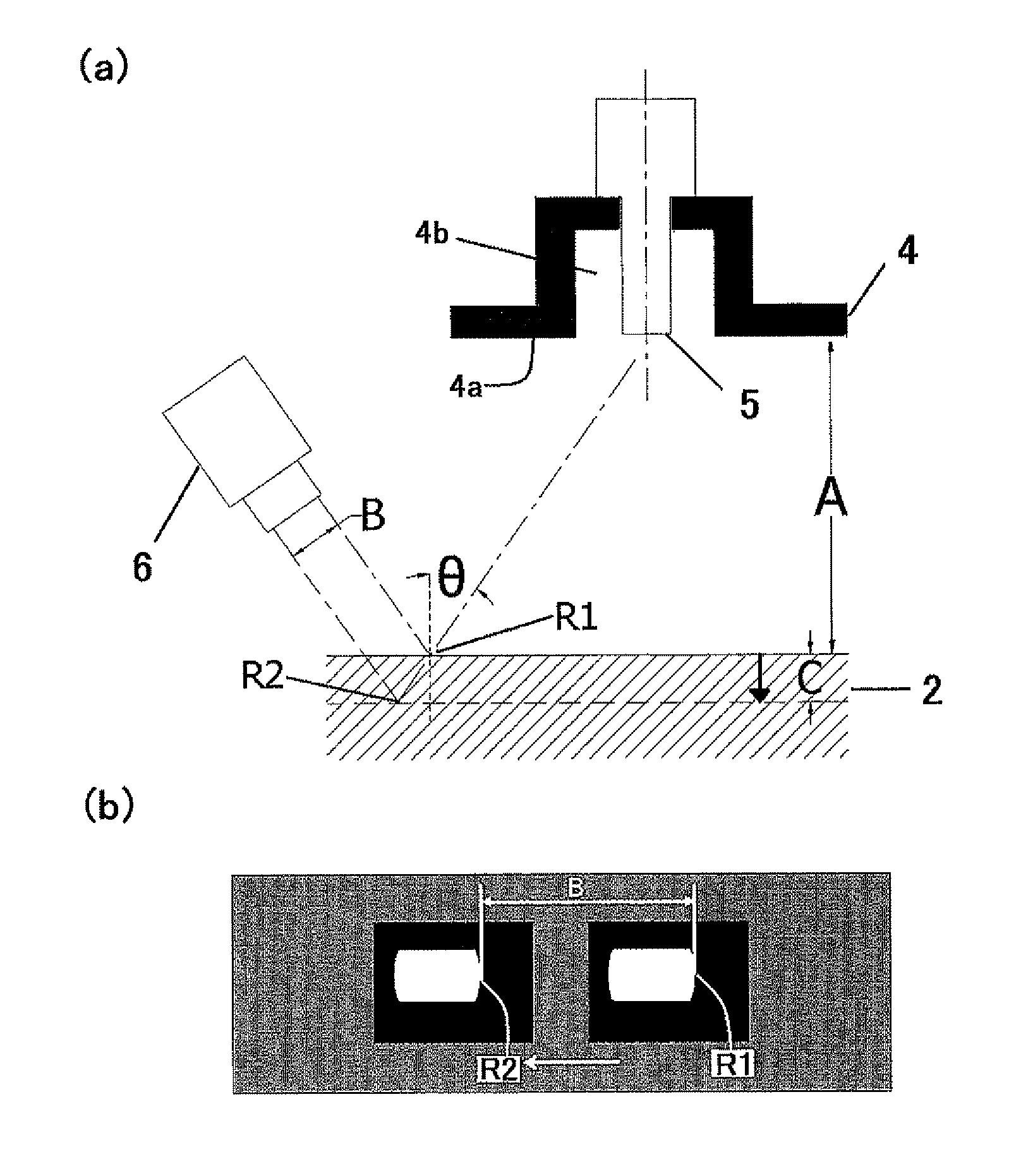
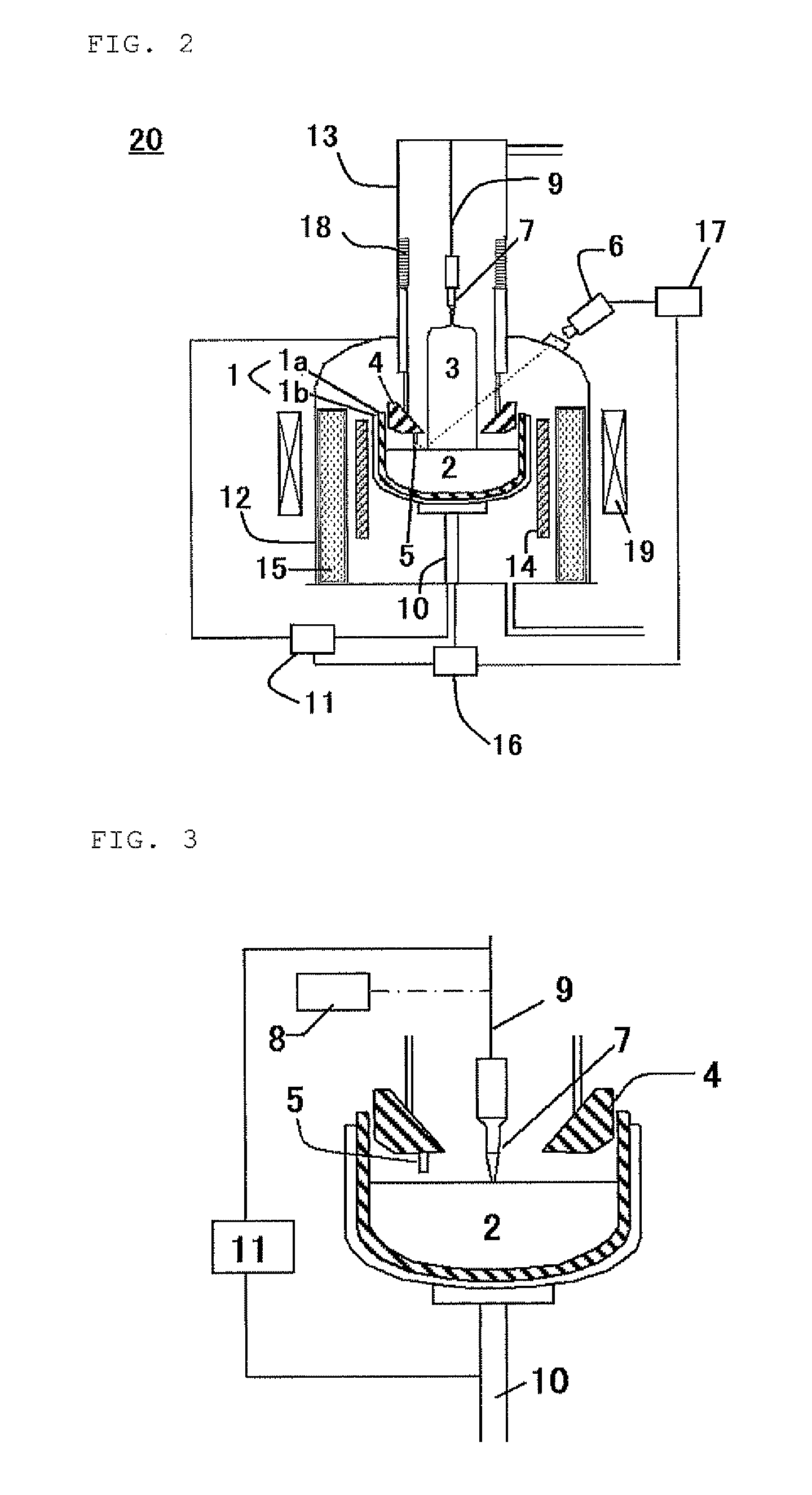
[0080]The silicon single crystal manufacturing apparatus 20 shown in FIG. 2 was used. First, with the heat shielding member 4, used for a long time, having scattered melts attached thereon, the concavity 4b was formed on the lower end surface 4a of the heat shielding member and the criterion reflector 5 is provided inside the concavity. In the used criterion reflector 5, white quartz was attached to the tip of a hard transparent quartz rod. Next, a polycrystalline silicon raw material of 340 kg was charged into a 800 mm diameter quartz crucible 1a (for pulling a 300 mm diameter silicon single crystal). The polycrystalline silicon raw material was melted with the heater 14 and a horizontal magnetic field of 4000 G at its center was then applied with the magnet 19.

[0081]The DPM was then actually measured by using the seed crystal 7. In this measurement, the position of the lower end of the seed crystal 7 was detected as the criterion position with the criterion position detector 8 as ...

example 2

[0087]A silicon single crystal 3 was pulled in the same conditions as Example 1 except for controlling the DPM. As described above, the DPM preferably varies continuously in crystal manufacture to increase the defect-free crystal region in the pulled silicon single crystal. In view of this, the silicon single crystal 3 was pulled while the crucible position was controlled with the crucible position control unit 16 so as to obtain a DPM of most preferable pattern in the same conditions as Example 1.

example 3

[0090]A silicon single crystal 3 was pulled and the DPM was measured in the same conditions as Example 1 except for using a new heat shielding member.


PUM

PropertyMeasurementUnit
horizontal magnetic fieldaaaaaaaaaa
diameteraaaaaaaaaa
diameteraaaaaaaaaa

Abstract

A method for measuring a distance between a lower end surface of a heat shielding member including a criterion reflector inside a concavity on the lower end surface and a surface of a raw material melt includes: a silicon single crystal is pulled by the Czochralski method while a magnetic field is applied to the raw material melt in a crucible, measuring the distance between the lower end surface of the heat shielding member and the surface of the raw material melt and observing a position of a mirror image of the criterion reflector with a fixed point observation apparatus; and measuring a movement distance of the mirror image with the apparatus and calculating the distance between the lower end surface of the heat shielding member and the surface of the raw material melt from the movement distance of the image and the measured distance.

Description

TECHNICAL FIELD[0001]The present invention relates to a method for measuring a distance between a lower end surface of a heat shielding member located above the surface of the raw material melt and a surface of a raw material melt when a silicon single crystal is pulled from the raw material melt in a crucible by the Czochralski method, and a method for controlling the distance.BACKGROUND ART[0002]The Czochralski method (CZ method), in which a silicon single crystal is grown and pulled from a raw material melt in a quartz crucible, has been widely implemented as a method for manufacturing a silicon single crystal for use in fabrication of a semiconductor device. In the CZ method, a seed crystal is dipped into the raw material melt (silicon melt) in the quartz crucible under an inert gas atmosphere, and the seed crystal is pulled while the quartz crucible and the seed crystal are rotated so that a silicon single crystal having a desired diameter is grown.[0003]In recent years, grown-...

Claims


Application Information

Patent Timeline
Patent Type & Authority Patents(United States)
IPC IPC(8): G06K9/00C03B29/06C30B15/26
CPCC03B29/06C30B29/06C30B15/26H01L21/02002
Inventor SUGAWARA, KOSEIURANO, MASAHIKOHOSHI, RYOJI
Owner SHIN-ETSU HANDOTAI CO LTD
Why Eureka
Try Eureka