Semiconductor apparatus

a technology of phase detection circuit and membrane, which is applied in the direction of pulse manipulation, pulse technique, instruments, etc., can solve the problems of increasing the time for amplification, reducing the potential difference between the sense nodes lsat and lsab at the end of the sampling period, etc., to suppress the increase in the time of phase detection, prevent erroneous phase detection decisions, and high precision

Inactive Publication Date: 2014-11-25
LONGITUDE SEMICON S A R L
View PDF12 Cites 0 Cited by
  • Summary
  • Abstract
  • Description
  • Claims
  • Application Information

AI Technical Summary

Benefits of technology

[0039]Recently, with increase in the operating speed and lowering in the operating voltage of the semiconductor device, the amplitude of the external clock signals CK and / CK is becoming smaller. If the amplitude of the external clock signals CK and / CK is smaller, the gate-to-source voltage in the nMOS transistors M3 and M6 for the High level (VDD2) of the external clock signals CK and / CK in FIG. 5 becomes lower and the drain-to-source currents of the nMOS transistors M3 and M6 become smaller. That is, the current driving capability of the nMOS transistors M3 and M6 discharging the charge in the sense nodes LSAT and LSAB becomes smaller. The current driving capability of the nMOS transistors also becomes smaller by reduction in the transistor size with the progress in miniaturization in the semiconductor fabrication process.
[0046]According to the present invention, it is possible to prevent erroneous decision in phase detection to suppress the time of phase detection from increasing to provide a high precision phase detection circuit without protracting the sampling period.

Problems solved by technology

If the current driving capability of the nMOS transistors M3 and M6 becomes smaller, there is raised a problem that the potential difference between the sense nodes LSAT and LSAB at the end of the sampling period is decreased.
This leads to a problem that an erroneous amplification occurs, or the time for amplification is increased in the sense amplifier AMP.

Method used


Image

  • Semiconductor apparatus
  • Semiconductor apparatus
  • Semiconductor apparatus

Examples


Embodiment Construction

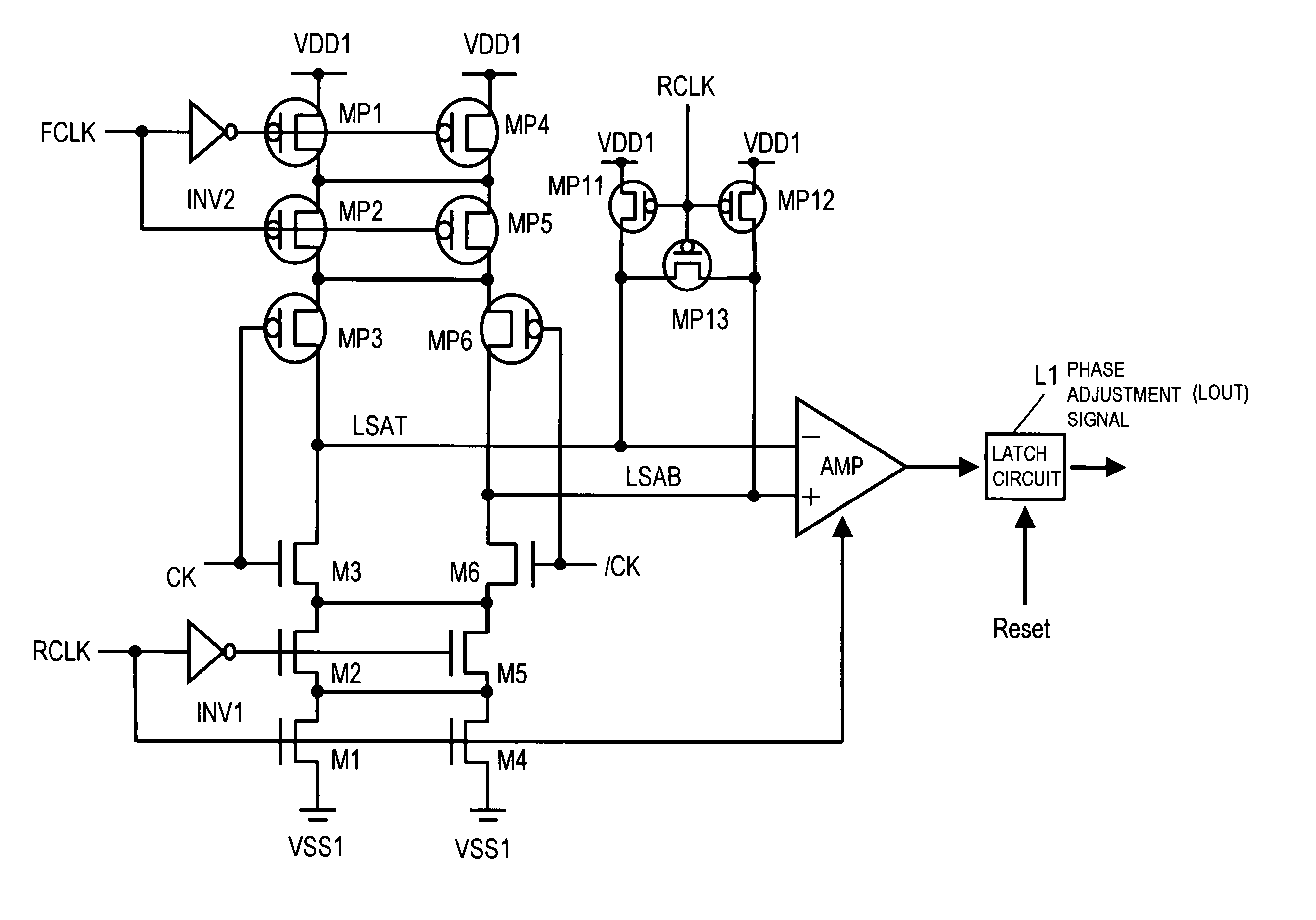
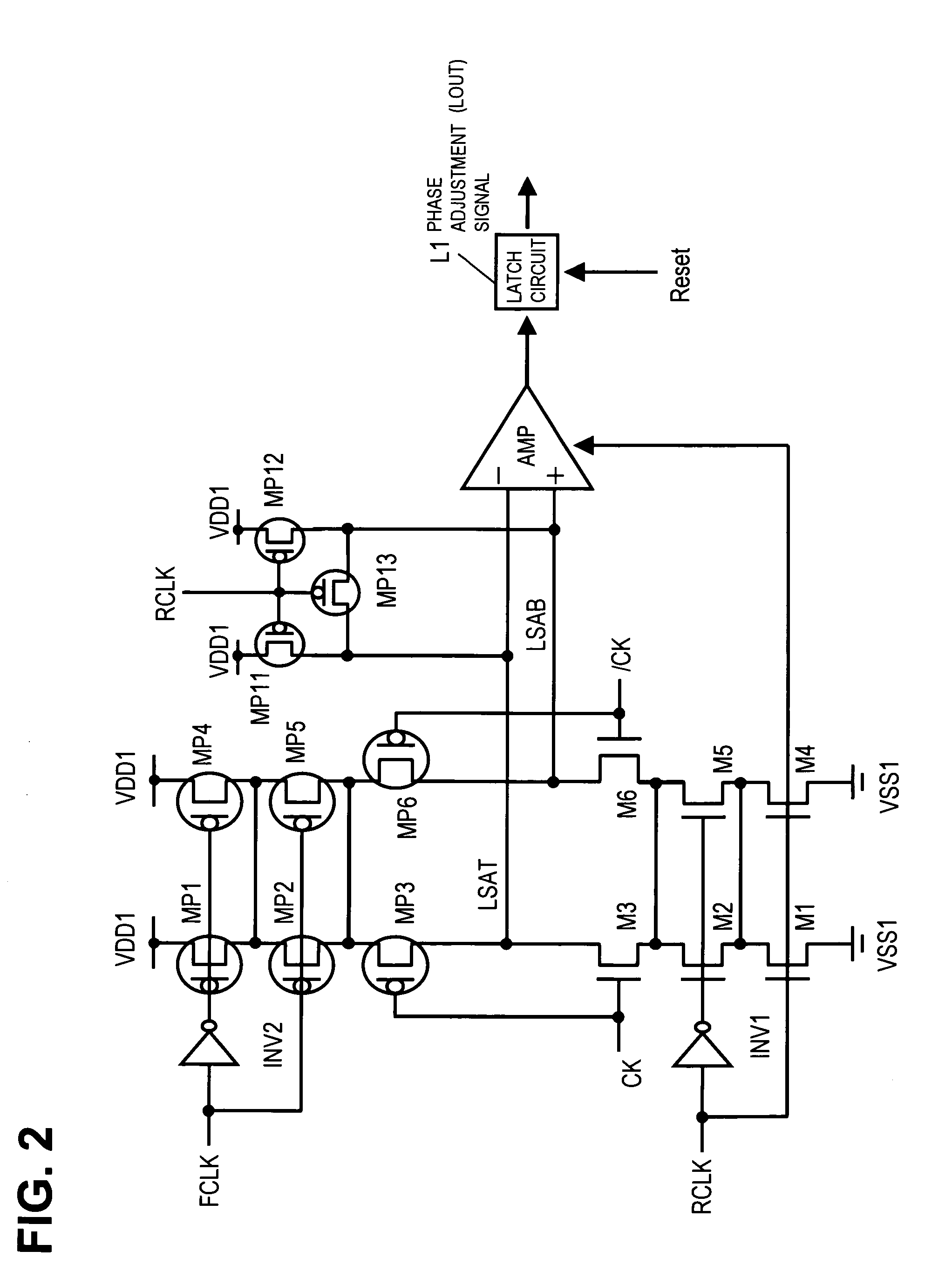
[0055]One of preferred modes of the present invention will now be described. A phase detection circuit arranged in a semiconductor device according to the present invention includes a path for charging sense nodes configured for phase detection and a path for discharging the sense nodes. The sense nodes include first and second sense nodes (LSAT, LSAB).

[0056]The discharge path for the first and second sense nodes (LSAT, LSAB) includes two sets of first, second and third transistors (M1, M2, M3) and (M4, M5, M6) connected in series between a first power supply (VSS1) and the first and second sense nodes (LSAT, LSAB), respectively. The control terminals of the first transistor pair (M1, M4) on the discharge path of the first and second sense nodes receive a first signal (RCLK) in common. The control terminals of the second transistor pair (M2, M5) of the discharge path of the first and second sense nodes receive in common a signal output from a first inverter (INV1) inverting the firs...


PUM


Abstract

In a semiconductor device, there are provided first to third pairs of nMOS transistors between a GND and two sense nodes and first to third pairs of pMOS transistors between the two sense nodes and the power supply. A first internal clock signal and its inverted signal are supplied to gates of the first pair of nMOS transistors and the second pair of nMOS transistors, respectively. Complementary external clock signals are supplied to the gates of the third pairs of nMOS transistors and the third pairs of pMOS transistors. An inverted version of a second internal clock signal and the second internal clock signal are supplied to gates of the first and second pairs of pMOS transistors. The two sense nodes are connected to inputs of a differential amplifier. The output of the differential amplifier is latched by a latch circuit. An equalizing circuit precharges / equalizes the two sense nodes.

Description

[0001]This Application is a Continuation Application of U.S. patent application Ser. No. 12 / 871,564, filed on Aug. 30, 2010, now U.S. Patent No. tbd.TECHNICAL FIELDReference to Related Application[0002]This application is based upon and claims the benefit of the priority of Japanese patent application No. 2009-198794, filed on Aug. 28, 2009, the disclosure of which is incorporated herein in its entirety by reference thereto.This invention relates to a semiconductor device and, more particularly, to a semiconductor device having a phase detection circuit.BACKGROUND[0003]Recently, a synchronous memory which performs an operation synchronized with a clock signal, has come into widespread use as a main memory of, for example, a personal computer. In particular, in a clock-synchronous memory such as a DDR (Double Date Rate) memory, input / output data need to be correctly synchronized with respect to an external clock signal. Hence, a DLL (Delay Lock Loop) circuit that generates an interna...

Claims


Application Information

Patent Timeline
Patent Type & Authority Patents(United States)
IPC IPC(8): G01R25/00H03D13/00H03L7/081H03L7/085G11C7/22H03K5/24
CPCH03L7/0816H03K5/249H03L7/0814G11C7/222H03L7/085
Inventor KUROKI, KOJITAKISHITA, RYUJI
Owner LONGITUDE SEMICON S A R L
Why Eureka
Try Eureka