Method of maintaining a memory state

a memory state and memory technology, applied in the field of methods, can solve the problems of many barriers to practical implementation of 3d stacked chips, copper or aluminum wiring levels, and deformation of the performance of the wires (interconnects) that connect together transistors, and achieve the effect of reducing the number of transistors

Inactive Publication Date: 2014-12-02
MONOLITHIC 3D
View PDF630 Cites 65 Cited by
  • Summary
  • Abstract
  • Description
  • Claims
  • Application Information

AI Technical Summary

Benefits of technology

[0014]In one aspect, a method of maintaining a memory state of a 3D memory, wherein said memory comprises at least a first cell and a second cell overlying said first cell, the method comprising: applying a back-bias to said first cell and said second cell without interrupting data access to said memory, and generating at least two stable floating body charge levels of said memory state.

Problems solved by technology

However, wires (interconnects) that connect together transistors degrade in performance with “scaling”.
However, there are many barriers to practical implementation of 3D stacked chips.
Copper or Aluminum wiring levels, in fact, can get damaged when exposed to temperatures higher than ˜400° C. If one would like to arrange transistors in 3 dimensions along with wires, it has the challenge described below.
When the Top Transistor Layer is constructed using Temperatures higher than 700° C., it can damage the Bottom Wiring Layer.Due to the above mentioned problem with forming transistor layers above wiring layers at temperatures lower than 400° C., the semiconductor industry has largely explored alternative architectures for 3D stacking.
Unfortunately, the size of Contacts to the other Layer is large and the number of these Contacts is small.
This low connectivity between layers is because of two reasons: (i) Landing pad size needs to be relatively large due to alignment issues during wafer bonding.
Etching deep holes in silicon with small lateral dimensions and filling them with metal to form TSVs is not easy.
Therefore, connectivity between two wafers is limited.
Unfortunately, however, almost all semiconductor devices in the market today (logic, DRAM, flash memory) utilize horizontal (or planar) transistors due to their many advantages, and it is difficult to convince the industry to move to vertical transistor technology.
A process flow is utilized to transfer this top transistor layer atop the bottom wiring and transistor layers at temperatures less than 400° C. Unfortunately, since transistors are fully formed prior to bonding, this scheme suffers from misalignment issues.
While Topol describes techniques to reduce misalignment errors in the above paper, the techniques of Topol still suffer from misalignment errors that limit vertical contact dimensions between two chips in the stack to >130 nm, and; hence, limits device density.
Unfortunately, however, these technologies have higher defect density compared to standard single crystal silicon and do not provide a mono-crystalline stacked layer or layers.
This higher defect density degrades transistor performance and device yield.
However, the approach described by Hubert has some challenges including the use of difficult-to-manufacture nanowire transistors, higher defect densities due to formation of Si and SiGe layers atop each other, high temperature processing for long times, difficult manufacturing, etc.

Method used


Image

  • Method of maintaining a memory state
  • Method of maintaining a memory state
  • Method of maintaining a memory state

Examples


Embodiment Construction

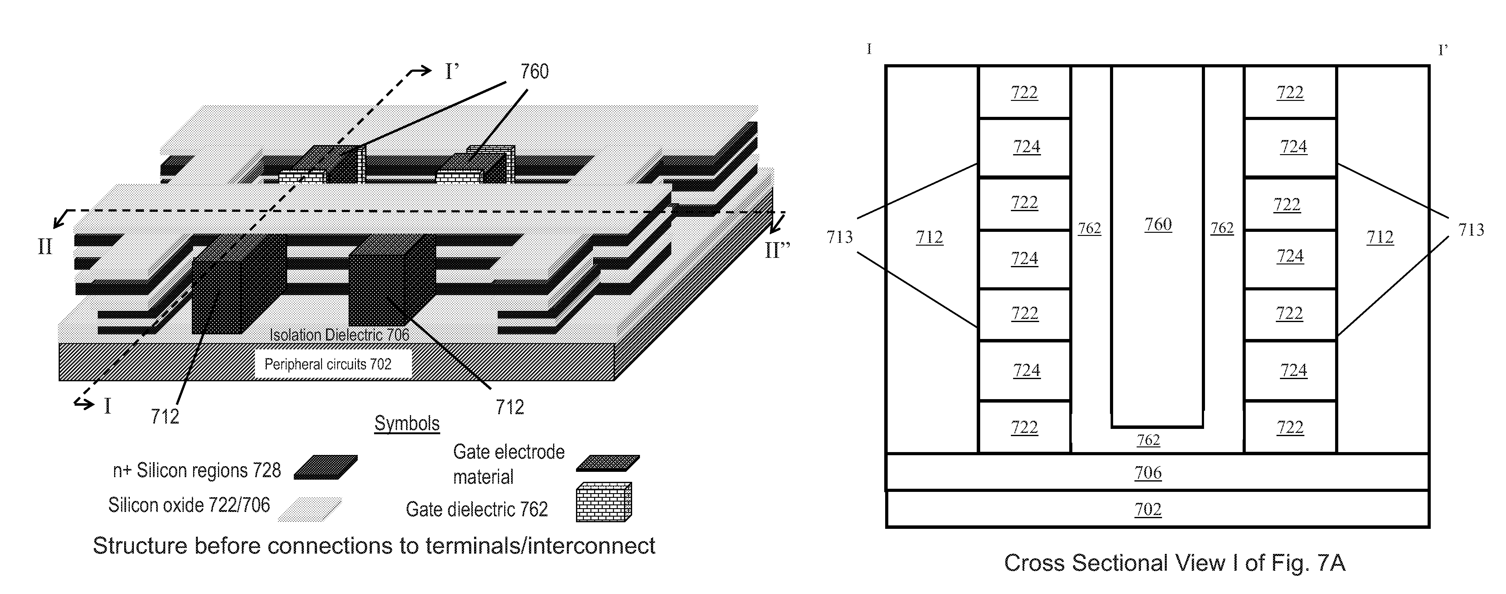
[0042]Embodiments of the invention are now described with reference to the indicated figures, it being appreciated that the figures illustrate the subject matter not to scale or to measure. Many figures describe process flows for building devices. These process flows, which may be a sequence of steps for building a device, may have many structures, numerals and labels that may be common between two or more adjacent steps. In such cases, some labels, numerals and structures used for a certain step's figure may have been described in previous steps' figures.

[0043]The entirety of U.S. Pat. No. 8,379,458 and U.S. Pat. No. 8,273,610 are incorporated herein by reference.

Section 1: Monolithic 3D DRAM.

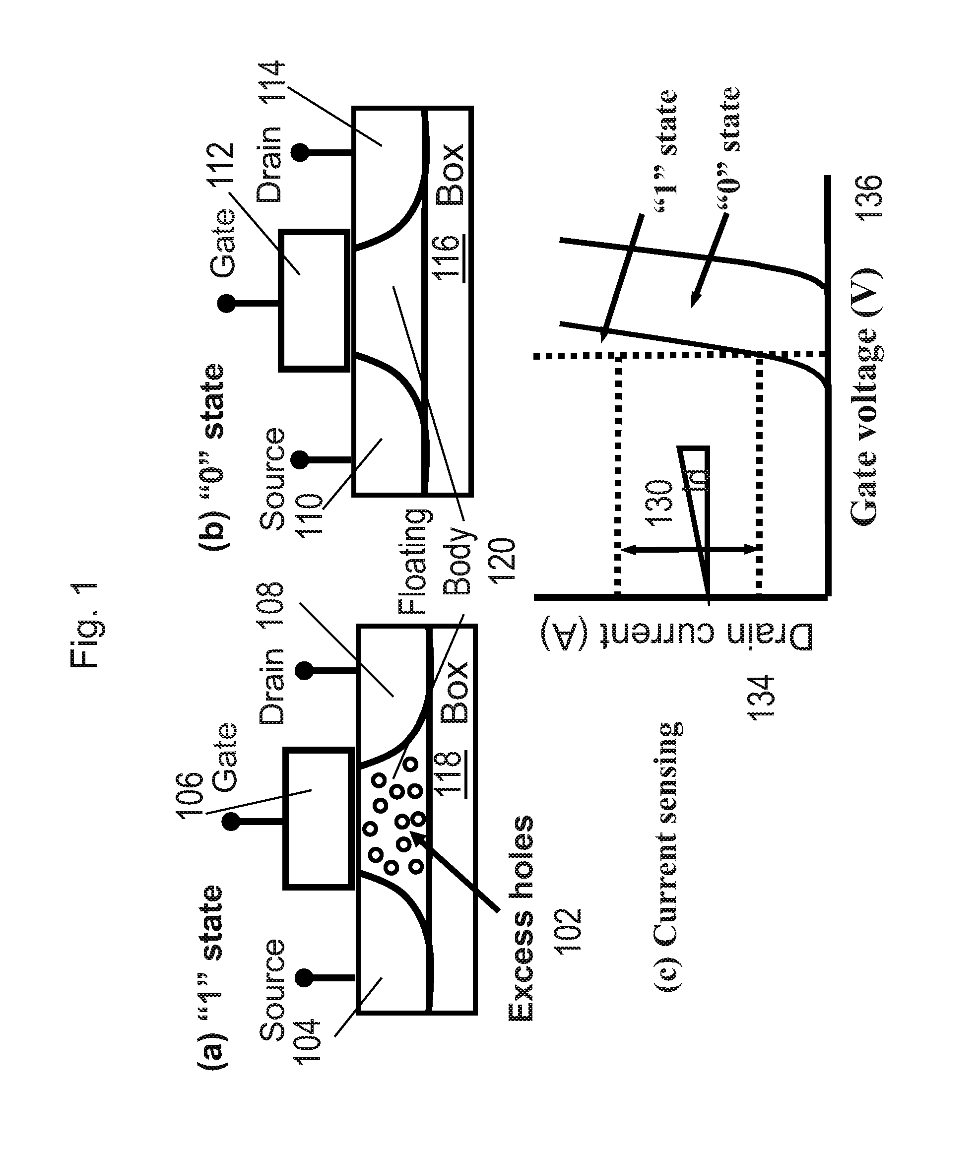
[0044]This Section describes some novel monolithic 3D Dynamic Random Access Memories (DRAMs). Some embodiments of this invention may involve floating body DRAM. Background information on floating body DRAM and its operation is given in “Floating Body RAM Technology and its Scalability to 32 nm...


PUM


Abstract

A method of maintaining a memory state of a 3D memory, wherein the memory includes at least a first cell and a second cell overlying the first cell, the method including: applying a back-bias to the first cell and the second cell without interrupting data access to the memory, and generating at least two stable floating body charge levels of the memory state.

Description

BACKGROUND OF THE INVENTION[0001]1. Field of the Invention[0002]This invention relates to the field of monolithic 3D integration to semiconductor chips performing logic and / or memory functions.[0003]2. Discussion of Background Art[0004]Over the past 40 years, the microelectronic industry has seen a dramatic increase in functionality and performance of Integrated Circuits (ICs). This has largely been due to the phenomenon of “scaling” i.e. component sizes within ICs have been reduced (“scaled”) with every successive generation of technology. There are two main classes of components in Complimentary Metal Oxide Semiconductor (CMOS) ICs, namely transistors and wires. With “scaling”, transistor performance and density typically improve and this has contributed to the previously-mentioned increases in IC performance and functionality. However, wires (interconnects) that connect together transistors degrade in performance with “scaling”. The situation today is that wires dominate performa...

Claims


Application Information

Patent Timeline
Patent Type & Authority Patents(United States)
IPC IPC(8): G11C16/02G11C16/04
CPCG11C16/02H01L27/115G11C11/404G11C11/4097G11C11/412G11C16/0483G11C2213/71H01L27/10802H01L29/78H01L29/7841H10B12/20H10B10/12H10B43/20H10B69/00H10B63/30
Inventor OR-BACH, ZVIWIDJAJA, YUNIARTO
Owner MONOLITHIC 3D
Why Eureka
Try Eureka