Organic light-emitting compound and organic light-emitting device including the same

a technology of organic light-emitting devices and compounds, which is applied in the direction of organic semiconductor devices, organic chemistry, natural mineral layered products, etc., can solve the problems of poor thermal stability of glass transition devices, high driving voltages, and significantly higher current efficiency, so as to improve luminescent efficiency and lifetime.

Active Publication Date: 2014-12-30
SAMSUNG DISPLAY CO LTD +1
View PDF10 Cites 2 Cited by
  • Summary
  • Abstract
  • Description
  • Claims
  • Application Information

AI Technical Summary

Benefits of technology

[0012]Embodiments of the present invention are directed to a novel organic light-emitting compound with a rigid backbone having improved luminescent efficiency and lifetime as compared with existing host materials, as well as appropriate color coordinates. Other embodiments of the present invention are directed to high-efficiency, long lifetime organic light-emitting devices using the organic light-emitting compound.

Problems solved by technology

Although they have advantageous light-emitting characteristics, these existing luminescent materials have low glass transition temperatures and poor thermal stability, and thus may deteriorate during high-temperature deposition processes conducted under vacuum.
In practice, OLEDs using common phosphorescent (host) materials, such as BAlq or CBP, may have higher driving voltages, but considerably higher current efficiency (cd / A), as compared with OLEDs using fluorescent materials, and thus are not advantageous in terms of power efficiency (Im / w).
OLEDs using such existing host materials are also not satisfactory in terms of lifetime.

Method used


Image

  • Organic light-emitting compound and organic light-emitting device including the same
  • Organic light-emitting compound and organic light-emitting device including the same
  • Organic light-emitting compound and organic light-emitting device including the same

Examples


example 1

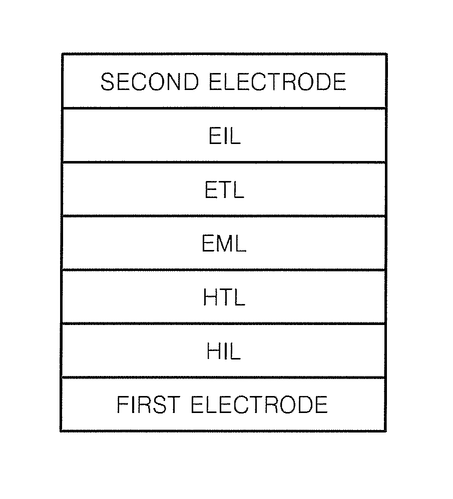
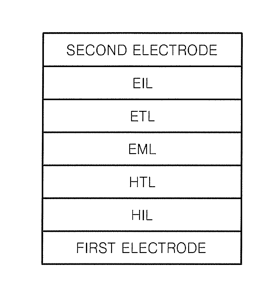
[0240]To manufacture an anode, a corning 15 Ω / cm2 (500 Å) ITO glass substrate was cut to a size of 50 mm×50 mm×0.5 mm and then sonicated in isopropyl alcohol and pure water each for 10 minutes, and then cleaned by irradiation with ultraviolet rays for 10 minutes and exposure to ozone. The resulting glass substrate was loaded into a vacuum deposition device.

[0241]Then, 2-TNATA, which is a HIL material, was vacuum-deposited on the glass substrate to form a HIL having a thickness of about 600 Å. Then, 4,4′-bis[N-(1-naphthyl)-N-phenylamino]biphenyl (NPB), which is a hole transporting compound, was vacuum-deposited on the HIL to form a HTL having a thickness of about 300 Å.

[0242]

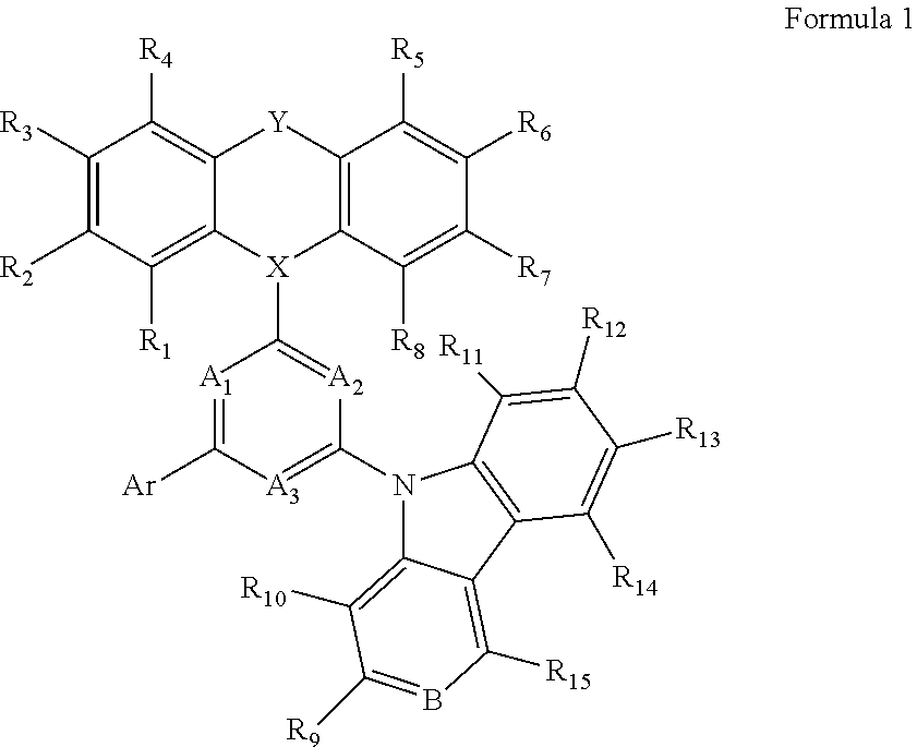
[0243]Then, a green fluorescent host Ir(PPy)3 and Compound 1 were deposited at the same time in a weight ratio of 13:87 on the HTL, to form an EML with a thickness of 300 Å. Next, Alq3 was deposited on the EML to form an ETL having a thickness of about 300 Å, and Al was deposited to a thickness of 1200 Å to form ...

example 2

[0245]An organic light-emitting device was manufactured in the same manner as in Example 1, except that Compound 5 instead of Compound 1 was used to form the EML.

[0246]The organic light-emitting device had a driving voltage of 4.2V at a current density of 5.9 mA / cm2, a high luminosity of 3500 cd / m2, color coordinates of (0.32, 0.63), and a luminescent efficiency of 58.9 cd / A.

example 3

[0247]An organic light-emitting device was manufactured in the same manner as in Example 1, except that Compound 8 instead of Compound 1 was used to form the EML.

[0248]The organic light-emitting device had a driving voltage of 4.0V at a current density of 5.9 mA / cm2, a high luminosity of 3500 cd / m2, color coordinates of (0.33, 0.63), and a luminescent efficiency of 60.7 cd / A.


PUM

PropertyMeasurementUnit
pressureaaaaaaaaaa
temperatureaaaaaaaaaa

Abstract

Embodiments of the present invention are directed to a compound represented by Formula 1 below and an organic light-emitting device including the compound.

Description

CROSS-REFERENCE TO RELATED PATENT APPLICATION[0001]This application claims priority to and the benefit of Korean Patent Application No. 10-2012-0071370, filed on Jun. 29, 2012 in the Korean Intellectual Property Office, the entire content of which is incorporated herein by reference.BACKGROUND[0002]1. Technical Field[0003]The present invention relates to a compound for organic light-emitting devices, and an organic light-emitting device including the compound.[0004]2. Description of the Related Art[0005]Organic light-emitting devices (OLEDs) are self-emitting devices having wide viewing angles, good contrast, quick response speeds, high brightness, and good driving voltage characteristics. Also, OLEDs can provide multicolored images.[0006]A typical OLED has a structure including a substrate, and an anode, a hole transport layer (HTL), an emission layer (EML), an electron transport layer (ETL), and a cathode sequentially stacked on the substrate. In this regard, the HTL, the EML, and...

Claims


Application Information

Patent Timeline
Patent Type & Authority Patents(United States)
IPC IPC(8): H01L51/00C07D413/14C07D417/14C07D471/04
CPCH01L51/5016H01L51/0085H01L2251/308H01L51/0081H01L51/0071H01L51/0067H01L51/0072C07D417/14C07D413/14C07D471/04H01L51/5012H01L51/0032C09K11/06C09K2211/1037C09K2211/1044C09K2211/1059C09K2211/1029C09K2211/1033H10K99/00H10K85/654H10K85/657H10K85/6572H10K85/324H10K85/342H10K50/11H10K2101/10H10K2102/103H10K85/00H10K85/649H10K50/15H10K50/16H10K50/17H10K50/171
Inventor LEE, JUNG-SUBYANG, SEUNG-GAK
Owner SAMSUNG DISPLAY CO LTD
Why Eureka
Try Eureka