Method of testing a semiconductor package

a technology of semiconductor chips and packages, applied in the field of semiconductor package testing, can solve the problems of increasing heat stress and warpage phenomenon generated by the mismatch of ctes of the smaller semiconductor chip and the larger substrate, reducing reliability between the semiconductor chip and the substrate, and causing reliability tests to fail accordingly. , the effect of reducing equipment costs and reducing fabrication costs

Active Publication Date: 2015-03-24
SILICONWARE PRECISION IND CO LTD
View PDF6 Cites 0 Cited by
  • Summary
  • Abstract
  • Description
  • Claims
  • Application Information

AI Technical Summary

Benefits of technology

[0018]According to the present invention, since no substrate exists when the electrical test is performed, the interposer and the semiconductor chip can be tested directly. Therefore, bad semiconductor chip or interposer can be detected in an early stage, and the fabrication cost is thus reduced. According to the present invention, the interposer and the semiconductor chip may be considered as a semiconductor chip in a conventional flip-chip fabrication process, and can be fabricated by a conventional flip-chip fabrication machine. Therefore, the equipment cost is also reduced. According to the present invention, the warpage of the interposer is alleviated by planarizing the adhesive layer or providing an un-singulated interposer. Therefore, the yield of the attachment of the semiconductor chip to the interposer is increased.

Problems solved by technology

With the increase of the integrity of integrate circuits disposed on the semiconductor chip, the thermal stress and warpage phenomenon generated due to the mismatch of CTEs of the smaller semiconductor chip and the larger substrate are more and more severe.
As a result, the reliability between the semiconductor chip and the substrate is reduced, and a reliability test fails accordingly.
The larger the number of the chips is, the greater the area of the substrate becomes, which does not comply with the compact-sized and low-profiled requirements for modern electronic products.
Besides, the electrical test steps of the prior art take much time, and, as such, the overall throughput drops.
Therefore, how to solve the problems of the prior art is becoming an urgent issue in the art.

Method used


Image

  • Method of testing a semiconductor package
  • Method of testing a semiconductor package
  • Method of testing a semiconductor package

Examples


Embodiment Construction

[0022]The following illustrative embodiments are provided to illustrate the disclosure of the present invention, these and other advantages and effects can be apparently understood by those in the art after reading the disclosure of this specification. The present invention can also be performed or applied by other different embodiments. The details of the specification may be on the basis of different points and applications, and numerous modifications and variations can be devised without departing from the spirit of the present invention.

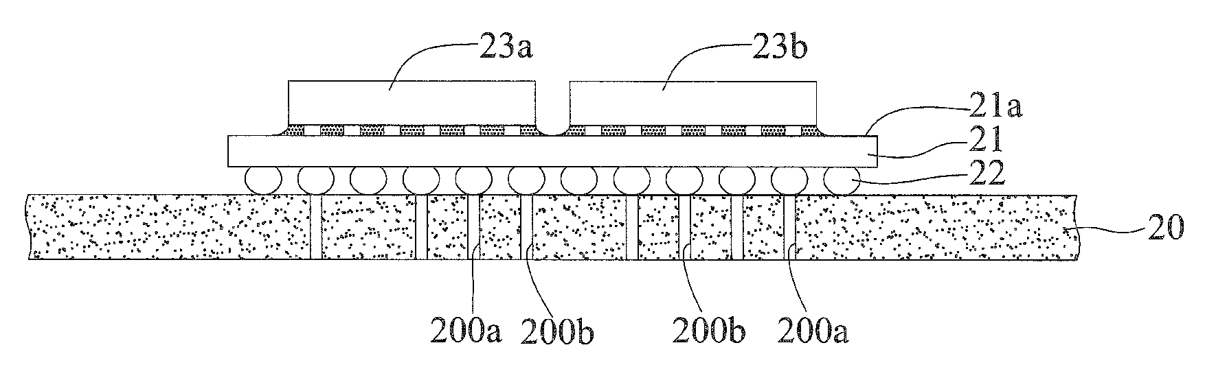
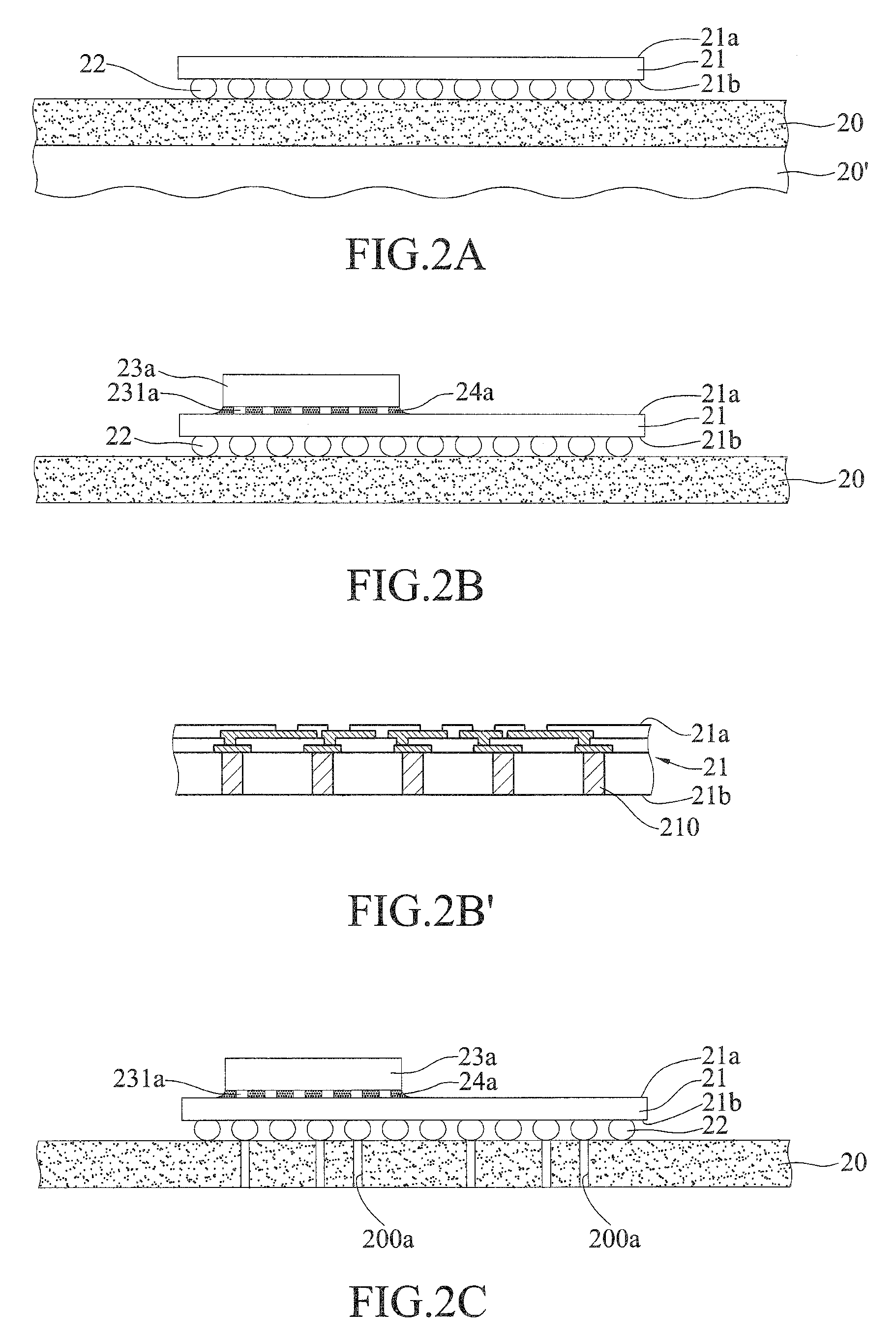
[0023]FIGS. 2A-2H are cross-sectional diagrams illustrating a method of testing a semiconductor package according to the present invention.

[0024]As shown in FIG. 2A, an interposer 21 is disposed on a top surface of an adhesive layer 20, and has a first surface 21a and a second surface 21b opposite to the first surface 21a. In an embodiment, the interposer 21 is made of a silicon-containing material. A plurality of conductive elements 22 is dispos...


PUM


Abstract

A method of testing a semiconductor package is provided, including: disposing at least an interposer on a top surface of an adhesive layer, the interposer having a first surface and a second surface opposite to the first surface, a plurality of conductive elements disposed between the second surface of the interposer and the adhesive layer; disposing at least a semiconductor chip on the first surface of the interposer, and performing an electrical test on the semiconductor chip via the conductive elements, wherein if there are a plurality of semiconductor chips that are disposed on the first surface of the interposer, the step of disposing the semiconductor chip and performing the electrical test on the semiconductor chip is iterated; and removing the adhesive layer. By using the method, the fabrication cost and equipment cost of the semiconductor package are reduced, and product yield is increased.

Description

CROSS-REFERENCES TO RELATED APPLICATIONS[0001]This application claims under 35 U.S.C. §119(a) the benefit of Taiwanese Application No. 101140943, filed Nov. 5, 2012, the entire contents of which is incorporated herein by reference.BACKGROUND OF THE INVENTION[0002]1. Field of the Invention[0003]This invention relates to semiconductor packages, and, more particularly, to a method of testing a semiconductor package.[0004]2. Description of Related Art[0005]Due to the capabilities of reducing a chip packaging area and shortening a signal transmission path, a flip-chip technique can be applied to a variety of chip packaging fields, such as a chip scale package (CSP), a direct chip attached (DCA) package, and a multi-chip module (MCM) package.[0006]In a flip-chip package fabrication process, since the coefficients of thermal expansion (CTE) of a semiconductor chip and a substrate that is greater than the semiconductor chip in area differ significantly, conductive bumps surrounding the semi...

Claims


Application Information

Patent Timeline
Patent Type & Authority Patents(United States)
IPC IPC(8): H01L21/66
CPCH01L22/14H01L22/20H01L2224/16225H01L2224/32225H01L2224/73204H01L2924/15174H01L2924/15311H01L2224/73253H01L2924/00H01L2924/37001H01L2224/83005H01L23/147H01L24/13H01L24/16H01L24/32H01L21/6836H01L24/73H01L24/81H01L24/83H01L24/97H01L25/0655H01L2224/131H01L2224/81005H01L2224/8181H01L2224/81815H01L2224/97H01L2924/157H01L2924/16195H01L23/367H01L23/49816H01L23/49827H01L2221/68331H01L2221/68381H01L2924/351H01L2924/12042H01L2924/00014H01L2924/00012H01L2224/83H01L2224/81
Inventor HUANG, PIN-CHENGLIN, CHUN-TANGTSENG, WEN-TSUNGLAI, YI-CHE
Owner SILICONWARE PRECISION IND CO LTD
Why Eureka
Try Eureka