Optical waveguide device

a waveguide and optical waveguide technology, applied in the direction of optical waveguide light guides, instruments, optics, etc., can solve the problems of increasing stress, reducing the bonding strength of the bonding, and not realizing the voltage reduction of the drive voltag

Inactive Publication Date: 2015-04-07
SUMITOMO OSAKA CEMENT CO LTD
View PDF16 Cites 3 Cited by
  • Summary
  • Abstract
  • Description
  • Claims
  • Application Information

AI Technical Summary

Benefits of technology

[0017]According to the invention, stress that occurs inside the optical waveguide substrate due to a difference in coefficient of thermal expansion may be reduced.

Problems solved by technology

However, in this configuration, since an electric field that is applied to the optical waveguide decreases due to the presence of the buffer layer, there is a disadvantage that voltage reduction of a drive voltage may not be realized.
However, in the configuration shown in FIG. 5, since the thickness of the adhesive layer 103 is large, the following problems occur.
First, if the thickness of the adhesive layer is large, the bonding strength thereof is apt to decrease.
Second, since the temperature is increased by ultraviolet irradiation or heating and lowered after being cured, stress occurs during the curing of the adhesive, and if the adhesive layer is thick, occurrence of the stress is apt to increase.
Third, manufacturing cost is increased, since a process for forming a thick adhesive layer involves difficult manufacturing steps, such as correcting of parallelism of a substrate and prevention of dripping.

Method used


Image

  • Optical waveguide device
  • Optical waveguide device
  • Optical waveguide device

Examples


first embodiment

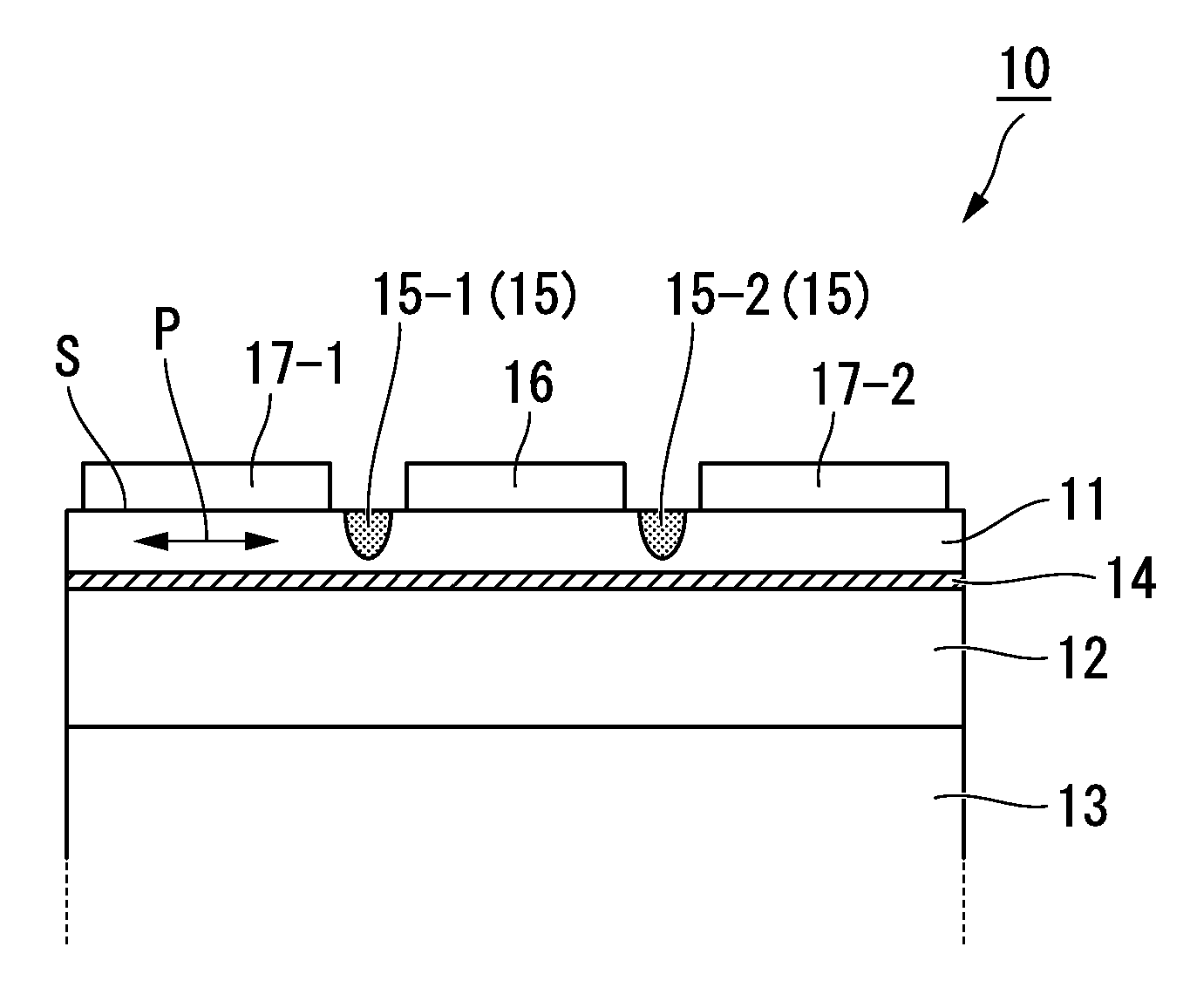
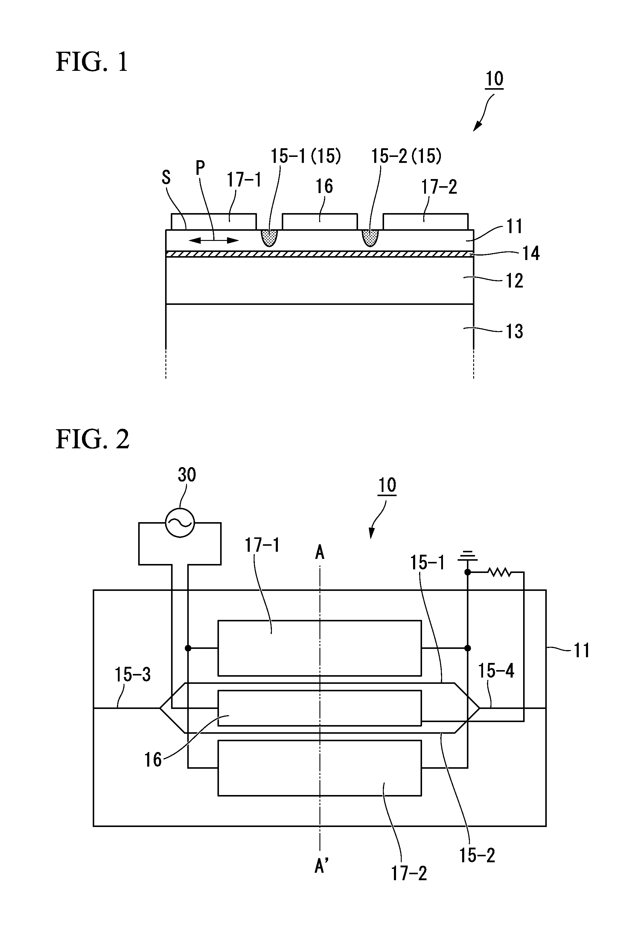
[0024]FIGS. 1 and 2 show a cross-sectional configuration view and a planar configuration view of a traveling-wave type optical modulator 10 that is an optical waveguide device according to a first embodiment of the invention, respectively. The cross-sectional configuration view of FIG. 1 illustrates a shape that is cut along a line A-A′ of the planar configuration view of FIG. 2.

[0025]In FIGS. 1 and 2, an optical modulator 10 includes an optical waveguide substrate 11 in which a Mach-Zehnder optical waveguide 15 is formed, a holding substrate 13 that holds the optical waveguide substrate 11, a liquid crystal polymer substrate 12 that is interposed between the optical waveguide substrate 11 and the holding substrate 13, an adhesive layer 14 that bonds and fixes the optical waveguide substrate 11 and the liquid crystal polymer substrate 12 to each other, and a signal electrode 16 and ground electrodes 17-1 and 17-2 that are formed on the optical waveguide substrate 11.

[0026]The optica...

second embodiment

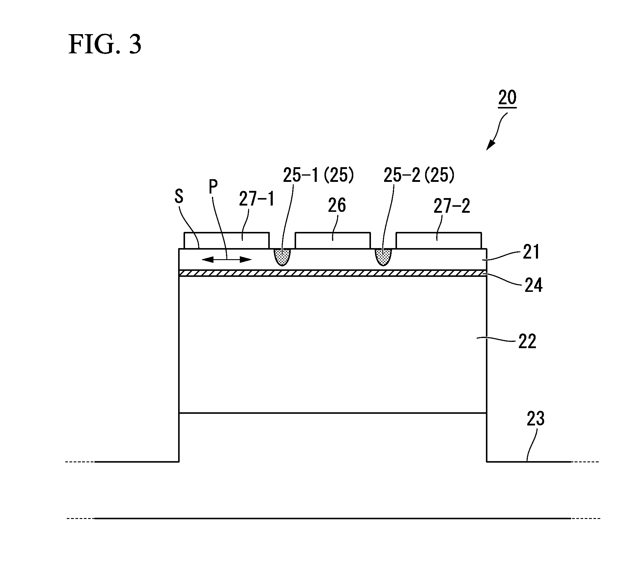
[0044]FIGS. 3 and 4 show a cross-sectional configuration view and a planar configuration view of a travelling-wave type optical modulator 20 that is an optical waveguide device according to a second embodiment of the invention, respectively. The cross-sectional configuration view of FIG. 3 illustrates a shape that is cut along a line A-A′ of the planar configuration view of FIG. 4.

[0045]In FIGS. 3 and 4, the optical modulator 20 includes an optical waveguide substrate 21 in which a Mach-Zehnder optical waveguide 25 is formed, a liquid crystal polymer substrate 22 that is a holding substrate that holds the optical waveguide substrate 21, an adhesive layer 24 that bonds and fixes the optical waveguide substrate 21 and the liquid crystal polymer substrate 22 to each other, a signal electrode 26 and ground electrodes 27-1 and 27-2 which are formed on the optical waveguide substrate 21, and a package housing 23 which fixes the liquid crystal polymer substrate 22.

[0046]The optical wavegui...


PUM

PropertyMeasurementUnit
thicknessaaaaaaaaaa
thicknessaaaaaaaaaa
thicknessaaaaaaaaaa

Abstract

Provided is an optical waveguide device capable of reducing stress that occurs inside an optical waveguide substrate due to a difference in a coefficient of thermal expansion. The optical waveguide device (10) includes an optical waveguide substrate (11) having a thickness of 30 μm or less, and a liquid crystal polymer substrate (12) which holds the optical waveguide substrate (11) and has permittivity lower than that of the optical waveguide substrate (11). The optical waveguide substrate (11) and the liquid crystal polymer substrate (12) are bonded to each other by an adhesive layer (14). Coefficients of thermal expansion of the optical waveguide substrate (11) and the liquid crystal polymer substrate (12) have anisotropy in each substrate plane, and a relative direction between the optical waveguide substrate (11) and the liquid crystal polymer substrate (12) is adjusted in such a manner that anisotropic axial directions of the optical waveguide substrate (11) and anisotropic axial directions the liquid crystal polymer substrate (12) are aligned.

Description

[0001]This application is a U.S. National Stage Application under 35 U.S.C. §371 of International Patent Application No. PCT / JP2012 / 061350 filed 27 Apr. 2012, which claims the benefit of priority to Japanese Patent Application No. 2011-102391 filed 28 Apr. 2011, the disclosures of all of which are hereby incorporated by reference in their entireties. The International Application was published in Japanese on 1 Nov. 2012 as WO 2012 / 147914.TECHNICAL FIELD[0002]The present invention relates to an optical waveguide device, and more specifically to, an optical modulator.BACKGROUND[0003]Recently, higher speed and capacity of an optical communication system has been progressing, and thus using a communication speed of 40 gigabit / second or higher per one wavelength has been considered practical. According to this, band-widening of the optical modulator, which is a basic component, has been demanded. A traveling-wave type optical modulator is an optical modulator that modulates optical waves...

Claims


Application Information

Patent Timeline
Patent Type & Authority Patents(United States)
IPC IPC(8): G02B6/10G02B6/12G02F1/03G02F1/035
CPCG02B6/12G02F1/0305G02F1/0356G02F2201/07G02F2201/54G02F2203/21G02F2202/022G02F2202/28
Inventor ICHIOKA, MASAYUKISAKUMA, MITSURUICHIKAWA, JUNICHIRO
Owner SUMITOMO OSAKA CEMENT CO LTD
Why Eureka
Try Eureka