
Dual port SRAM having reduced cell size and rectangular shape

a sram and cell technology, applied in the field of dual port srams, can solve the problems of degrading cell performance, memory cell creating additional problems, high wordline rc time constant, etc., and achieve the effect of improving performance, high performance and performing the function

Active Publication Date: 2015-04-14
STMICROELECTRONICS INT NV
View PDF5 Cites 39 Cited by
  • Summary
  • Abstract
  • Description
  • Claims
  • Application Information

AI Technical Summary

Benefits of technology

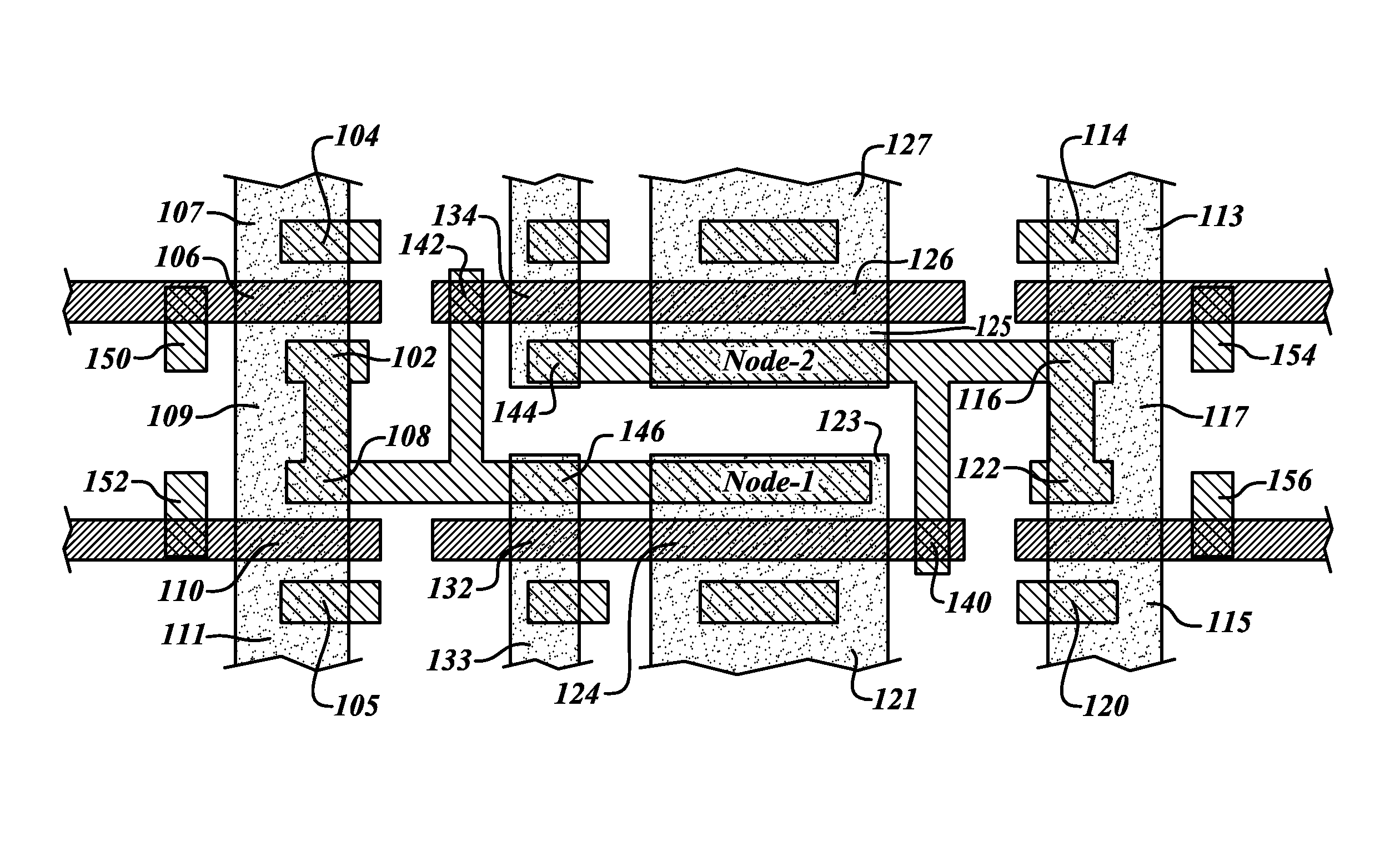
[0021]This particular arrangement has a number of advantageous. First, the active areas of the storage nodes can each be designed to better perform its respective function for the transistor of which is a drain. Since each of the active areas for the storage transistors are physically isolated from each other and is the active area for just a single transistor and is not part of the pass gates, the shape, size and to some extent, the location of each, can be selected to permit the transistor of which it is a part to best perform its function in the memory cell, whether that of a pull-up transistor, a pass gate or a pull-down transistor. Each of these transistors has a specific and width to length ratio that will provide better performance for a given size. The size each active area can therefore be selected to provide a very small memory cell and the shape and location selected for high performance without having to be concerned about the trade off of the performance of another transistor that may share the same active area. Similarly, the active area for the pass gates is physically separate from the active area of both the pull-up an pull-down transistors so that its size and shape can be selected to better perform the function of a pass gate without having to be concerned with the performance tradeoffs of having to design the active area to also function as part of the storage node transistors.
[0022]In one embodiment, metal 1, called M1, is a blanket layer deposited over exposed conductive layers without the use of contacts or vias. The layer, after being blanket deposited, if patterned and etched to remove it from all locations in which an electrical connection to M1 is not desired. This use of M1 provides full electrical connection of all internal routing of the memory cell without the use of contacts or vias, thus substantially reducing the size of the cell and increasing the performance in both speed and current carrying ability. In a preferred embodiment, M1 is deposited, patterned and etch in two different layers, each having the same material, but each creating patterns of perpendicular to each other.
[0023]The source power supply line, Vss is positioned in the center of the cell and coupled at two locations inside of each cell, to the sources of the pull down transistors. The sources of the two pull-down transistors are separate from each other and not in the same active area. The source power supply line is located at a position relative to the other power supply line, Vdd and to the bit lines that is can be made quite wide to provide lower resistance and faster speeds. The current carrying capability of Vss is high as compared to the bit lines to permit two different bit lines to access the data storage nodes, either concurrently or simultaneously, and still retain the correct data as valid. In addition, in one embodiment, the current carrying capability of Vdd is also high as compared to the bit lines to permit two different bit lines to access the data storage nodes, either concurrently or simultaneously without loss of data.
[0024]In one embodiment, the power supply lines Vss and Vdd are formed in different metal levels than either the bit lines or the word lines. This permits the power supply lines to made wider than would be permitted if they were in the same metal layers as either bit lines or the word lines. In one embodiment, the power supply lines are sufficiently wide and the cell is sufficiently compact that the bit lines overlay at least one portion of the supply lines and are electrically isolated from them by a low-K dielectric layer or layers.
[0025]The particular layout and sizing of the memory cell permits the memory cell for the dual port SRAM to have an aspect ratio of approximately 3. In some embodiments, the aspect ratio is 3.2 while in others, it is 2.85, both of which are approximately 3. In one embodiment, the aspect ratio is less than 2.5. Having a low aspect ratio, of about 3 or less improves the speed of memory cell for reading and writing while significantly reducing the RC delay in the various conductive lines.

Problems solved by technology

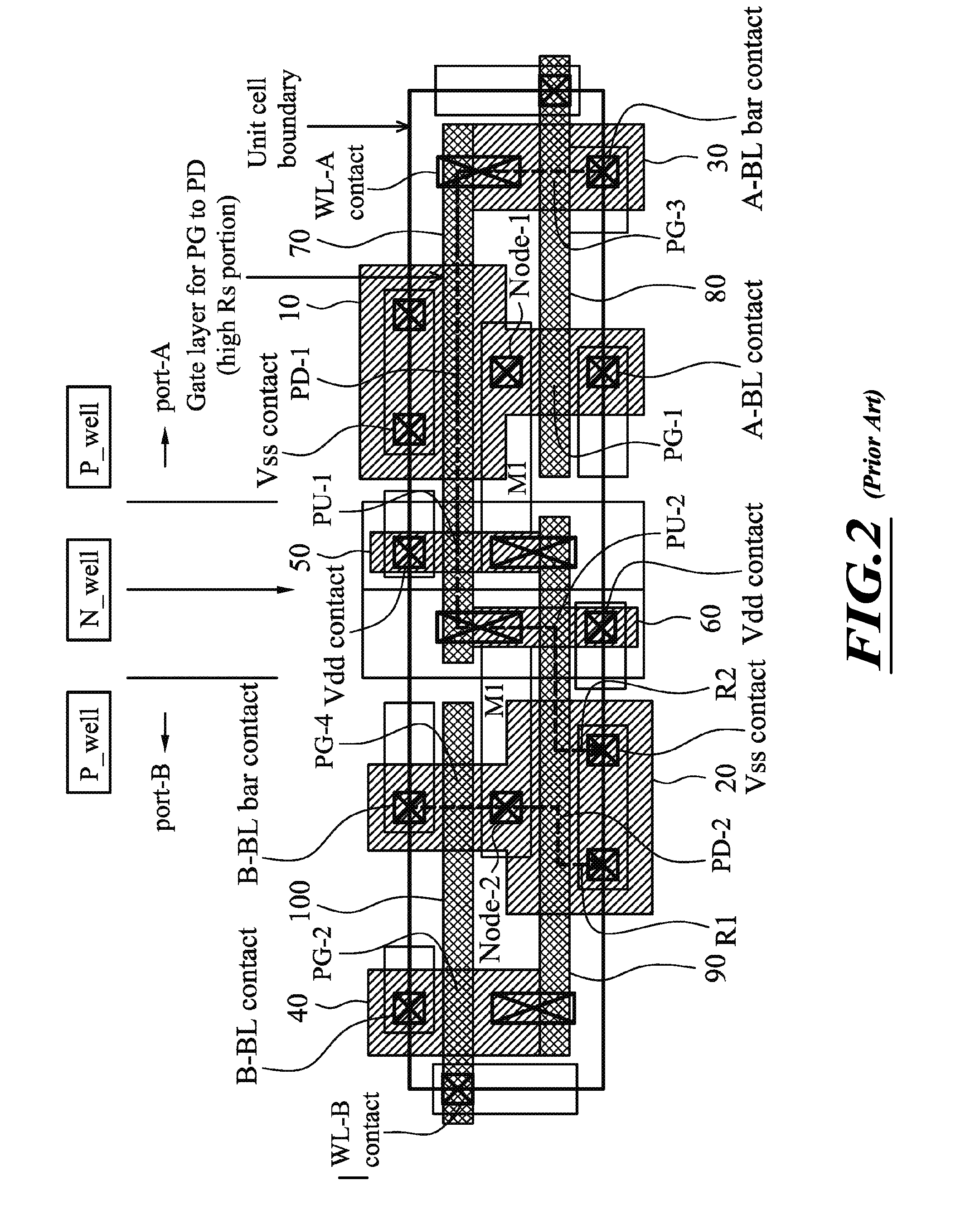
In a memory cell layout of this type, the performance is degraded due to a high wordline capacitance which results in a high wordline RC time constant.
Other features of the layout of the memory cell create additional problems.
The result will be rounded edges and that the available width of the transistor is reduce resulting in degraded cell performance.
In addition, if a misalignment occurs, the gate electrode of the PG transistors may not be in the expected location unless the width is increased.
This will result in a greater mismatch between the pass gates and the other transistors, thus significantly degrading SRAM cell performance.
In addition, there will be problems in current grabbing at the intersection junction.
Therefore, some portions of PD-1 and PD-2 will have greater current densities than other portions and significant problems further degrading performance and impacting the reliability.
In addition, junction linkage is also a problem in a cell layout of this type.
The extended current path, and having to pass through repeated contacts, contributes to a greater than 10% recurrent loss in device sizes of 28 nm with increasing losses at smaller sizes.
In addition, the isolated active regions of pass gates are also impacted by STI stress losses which are greater than 4% of the recurrent at the 28 nm device size.
The addition of two transistors makes his memory cells even larger and more difficult to construct in small geometries.
The design of '289 Liaw is difficult to construct in very small device sizes, such as 28 nm and 20 nm.
In addition, the 20 nm technology design rules prohibit two wordline connections at two polypitch heights, therefore his solution is unworkable for small memory cells.
A further problem is the use of metal 1 as the local interconnection to connect two fingers of the pull down transistors.
This additional routing requirement makes the cell incompatible with many other memory cells and other transistors to be made on the same device which may not permit use of metal 1 for local interconnects.
A yet additional problem is the high aspect ratio of the memory cell.

Method used


Image

  • Dual port SRAM having reduced cell size and rectangular shape
  • Dual port SRAM having reduced cell size and rectangular shape
  • Dual port SRAM having reduced cell size and rectangular shape

Examples


Embodiment Construction

[0042]A new layout is provided for a dual port memory cell as illustrated in FIGS. 6-13, an alternative embodiment of which is shown in FIGS. 14 and 15.

[0043]The figures as shown herein are generally to scale with respect to the specific layouts. Namely, the features as shown in the layouts of FIGS. 7-15 are examples that represent the actual relative dimensions of the structures in one embodiment and show the feature sizes relative to each other. Some variation may exist between the different features as shown in these embodiments and their sizes relative to each other, and still fall within use of the present invention since the scope of the invention is defined by the claims and not by the figures or the specification. Namely, the location and general shape of the structures as shown herein constitutes a novel layout with advantageous and unexpected properties. A layout of the type shown herein may have many different sizes of components in different sizes relative to each other ...


PUM


Abstract

A dual port SRAM has two data storage nodes, a true data and complementary data. A first pull down transistor has an active area that forms the drain region of the first transistor and the true data storage node that is physically isolated from all other transistor active areas of the memory cell. A second pull down transistor has an active area that forms the drain region of a second transistor that is the complementary data node that is physically isolated from all other transistor active areas of the memory cell.

Description

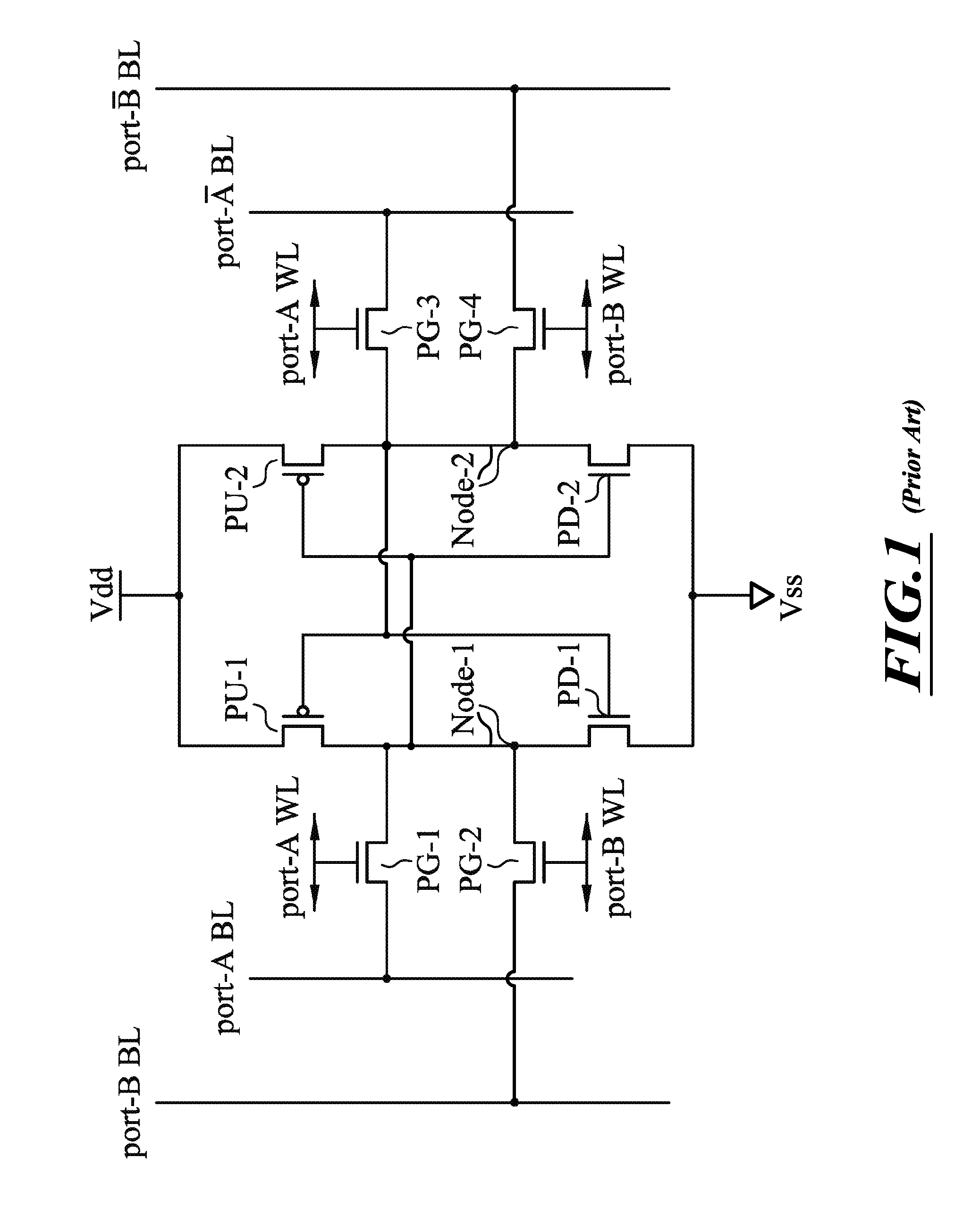
BACKGROUND[0001]1. Technical Field[0002]This invention relates to dual port SRAMs and, in particular, to a dual port SRAM having a reduced feature size in a rectangular-shaped cell layout.[0003]2. Description of the Related Art[0004]A dual port SRAM circuit is shown in FIG. 1 of a type well known in the art. Dual port SRAMs are particularly advantageous in certain types of memories to allow fast access for reading and writing. For example, dual port SRAMs may be used for the internal memory of a microprocessor in various stack registers. A dual port SRAMs is also frequently used in high speed communications, image processing, a FIFO and other circuits in which high speed and high reliability are required while accessing the memory cell through multiple ports during time periods which may overlap and even occur simultaneously. For these reasons, dual port SRAMs of the circuit type as shown in FIG. 1 have particular benefits across a wide range of products.[0005]Embedded SRAMs are par...

Claims


Application Information

Patent Timeline
Patent Type & Authority Patents(United States)
IPC IPC(8): H01L27/11
CPCH01L27/1104H01L27/11G11C11/412H01L27/0207H10B10/12H10B10/00
Inventor KUMAR, SHISHIRDIPTI, DIBYAMALINGE, PIERRE
Owner STMICROELECTRONICS INT NV
Learn More