Semiconductor package substrate and semiconductor package including the same

a technology of semiconductor package and substrate, applied in the direction of semiconductor/solid-state device details, semiconductor devices, electrical apparatus, etc., can solve the problems of rapid signal transmission loss in a specific frequency band, discontinuous coupling of metal layers, impedance mismatch, etc., to prevent impedance mismatch

Inactive Publication Date: 2015-04-28
SK HYNIX INC
View PDF6 Cites 0 Cited by
  • Summary
  • Abstract
  • Description
  • Claims
  • Application Information

AI Technical Summary

Benefits of technology

[0013]Various embodiments generally relate to a semiconductor package substrate capable of preventing impedance mismatch which occurs when pluralities of metal layers are coupled through a conductive via, and a semiconductor package having the same.

Problems solved by technology

However, when pluralities of metal layers are coupled through conductive vias, the metal layers may be discontinuously coupled.
However, the discontinuous coupling may cause impedance mismatch when a signal operating at a high frequency is transmitted.
However, when the substrate is used, a rapid signal transmission loss occurs in a specific frequency band, which is indicated by a thick line.
Such a loss may be caused by impedance mismatch of transmission lines.
This may cause signal delay.

Method used


Image

  • Semiconductor package substrate and semiconductor package including the same
  • Semiconductor package substrate and semiconductor package including the same
  • Semiconductor package substrate and semiconductor package including the same

Examples


Embodiment Construction

[0038]Hereinafter, various embodiments will be described with reference to accompanying drawings. However, the embodiments are for illustrative purposes only and are not intended to limit the scope of the invention. Also, the same reference numerals or the same reference designators may denote the same elements throughout the specification.

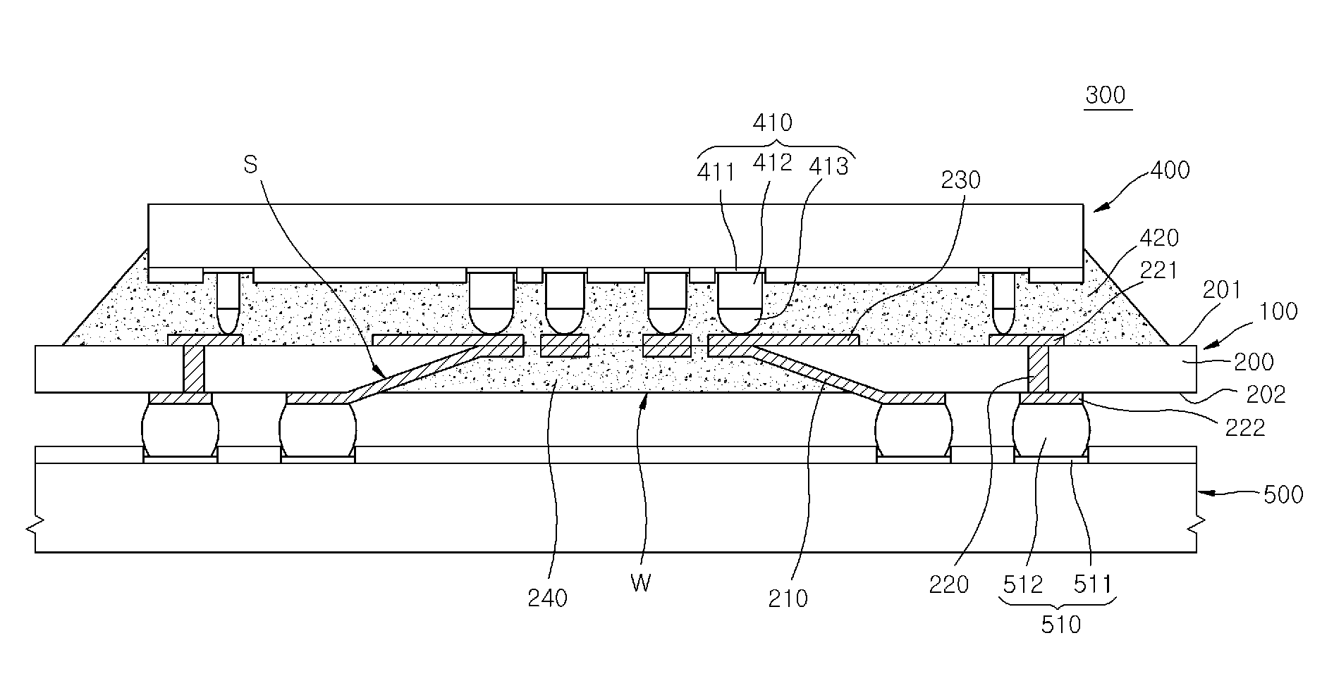
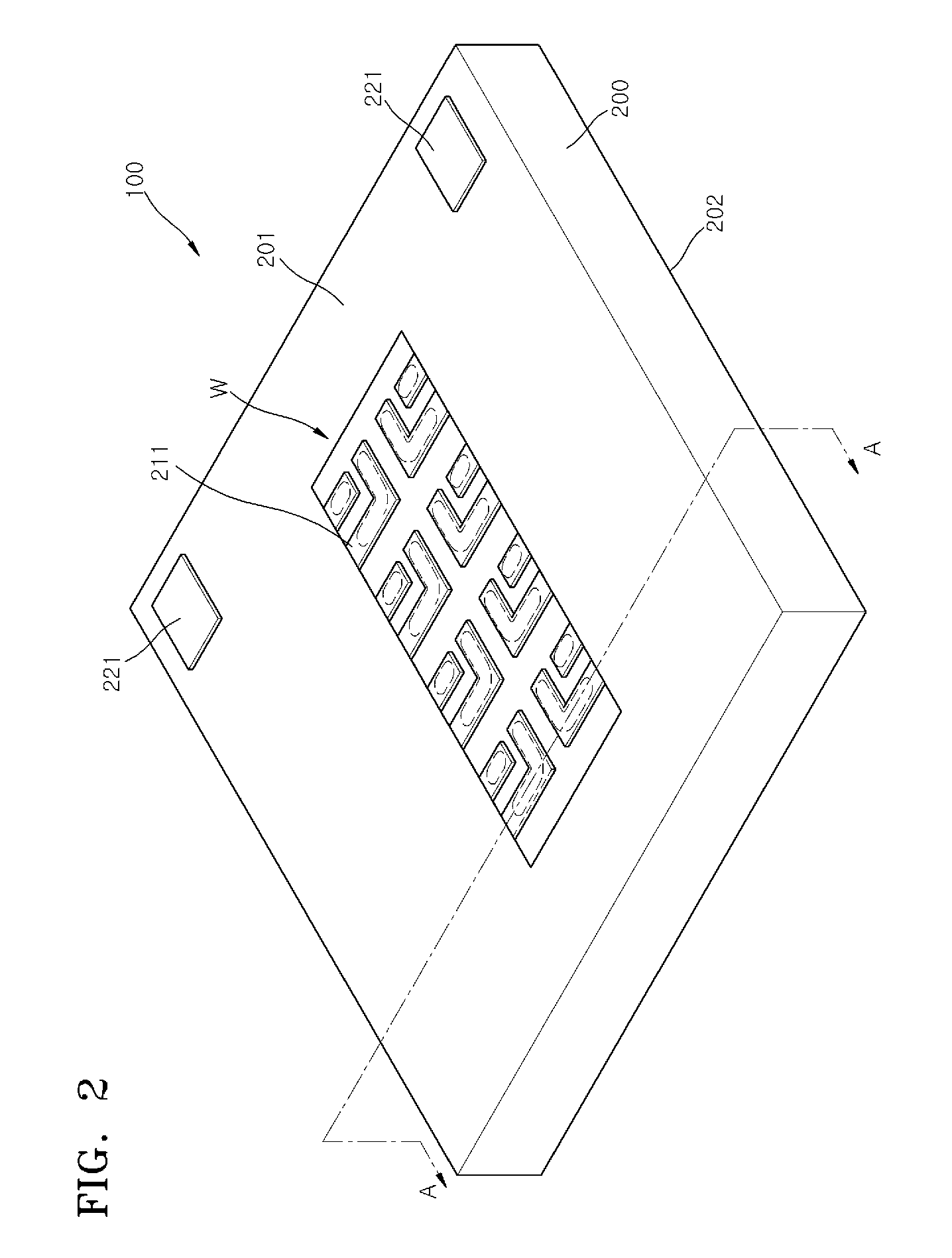
[0039]FIG. 2 is a front perspective view of a semiconductor package substrate in accordance with an embodiment. FIG. 3 is a rear perspective view of the semiconductor package substrate in accordance with an embodiment. FIG. 4 is a cross-sectional view taken along a line A-A′ of FIG. 2.

[0040]Referring to FIGS. 2 to 4, the semiconductor package substrate 100 in accordance with an embodiment may include a substrate body 200 having a front surface 201 having a semiconductor chip mounted thereon and a rear surface 202 coupled to a system substrate. The semiconductor chip may include a semiconductor device such as a memory device or logic device.

[0041]I...


PUM


Abstract

A semiconductor package substrate including a substrate body having a front surface configured for mounting a semiconductor chip on the front surface and a rear surface facing the front surface and comprising a window passing through the front and rear surfaces, the window having one or more surfaces inclined from the front surface toward the rear surface; and a conductive pattern arranged along an inclined surface of the window so as to extend from the front surface to the rear surface of the substrate body.

Description

CROSS-REFERENCES TO RELATED APPLICATIONS[0001]The present application claims priority under 35 U.S.C 119(a) to Korean Application No. 10-2011-0107107, filed on Oct. 19, 2011 in the Korean intellectual property Office, which is incorporated herein by reference in its entirety set forth in full.BACKGROUND[0002]1. Field of the Invention[0003]Various embodiments of the present disclosure relate to a substrate used for a semiconductor package and a semiconductor package including the same.[0004]2. Description of the Related Art[0005]With high performance of electric / electronic products and reduction in size and weight of electronic devices, it has become important to reduce the thickness of packages and increase the density of packages. With the increase in memory capacity of computers, notebooks, and mobile phones, the capacity of chips such as large-capacity RAM and flash memory has increased, but the size of packages has decreased. In order to implement such packages, research has bee...

Claims


Application Information

Patent Timeline
Patent Type & Authority Patents(United States)
IPC IPC(8): H01L23/48H01L23/52H01L29/40H01L23/00H01L23/13H01L23/367H01L23/498
CPCH01L23/13H01L24/17H01L23/3677H01L23/49827H01L2224/16225H01L2224/32225H01L2224/73204H01L2924/15311H01L23/49816H01L2924/00H01L23/12H01L23/48
Inventor KIM, JONG HOON
Owner SK HYNIX INC
Why Eureka
Try Eureka