Two-state negative feedback avalanche diode having a control element for determining load state

a negative feedback and diode technology, applied in the field of single-photon avalanche photodetectors, can solve the problems of runaway avalanche, easy detection of macroscopic current, and inability to combine high operational speed and wavelength range required for many applications of current spads

Active Publication Date: 2015-05-05
LG INNOTEK CO LTD
View PDF1 Cites 21 Cited by
  • Summary
  • Abstract
  • Description
  • Claims
  • Application Information

AI Technical Summary

Benefits of technology

[0021]In some embodiments, the control element provides a temporal delay appropriate for delayed switching of the load between its two states.

Problems solved by technology

Unfortunately, currently available SPADs do not have the combination of high operational speed and wavelength range required for many of these applications.
In Geiger-mode operation, a SPAD is “armed” by biasing it with a voltage that is above its breakdown voltage, which is the voltage bias level above which free-charge carrier generation can become self-sustaining and result in a run-away avalanche.
Arming a SPAD puts it in a meta-stable state in which absorption of a single photon can give rise to a runaway avalanche that results in an easily detectable macroscopic current.
Controlling voltage bias to arm and quench an APD is one of the primary challenges for Geiger-mode operation and the rate at which a single-photon detector can be operated is determined by (1) how quickly the APD can be quenched once a photon has been detected and (2) how quickly the APD can be re-armed once it has been quenched.
As a result, the detrapping of a carrier can result in a “false” electrical signal that occurs in the absence of photon absorption.
As a result, afterpulses degrade SPAD sensitivity.
Unfortunately, such an approach requires an undesirably long period of time when the single-photon detector is insensitive to incident photons.
Such approaches, however, have shown very limited success.
Elevating the temperature of an APD imposes a severe tradeoff by increasing the dark count rate while sub-bandgap illumination has not yet been shown to effectively induce carrier detrapping.
In addition, these approaches increase cost and complexity, making these approaches undesirable in many applications.
The stifling of trapped charges by lowering the temperature of a SPAD to “freeze” trapped charge carriers has not been successfully demonstrated.
In fact, for practical SPAD devices, this approach is likely to increase after-pulsing as temperature is reduced.
Further, if carrier freeze-out were successful, it is likely that at least some of the charge carriers associated with the dopant atoms would also be “frozen,” thus rendering the SPAD inoperable.
As a result, any capacitance associated with external electronics that adds to the capacitance of the SPAD itself is generally undesirable.
Moreover, the use of external circuitry generally involves significant complexity, and it can lead to additional undesirable parasitic elements in addition to the capacitance just described.
However, this legacy “negative feedback avalanche diode” (NFAD) is limited by an inherent tradeoff: a large feedback load is desired to promote rapid quenching, but a small feedback load is necessary to enable rapid re-arming.
In prior-art NFADs, a single feedback load value is chosen to balance this tradeoff between the timescales for quenching and re-arming and, therefore, overall device performance is necessarily compromised.

Method used


Image

  • Two-state negative feedback avalanche diode having a control element for determining load state
  • Two-state negative feedback avalanche diode having a control element for determining load state
  • Two-state negative feedback avalanche diode having a control element for determining load state

Examples


Embodiment Construction

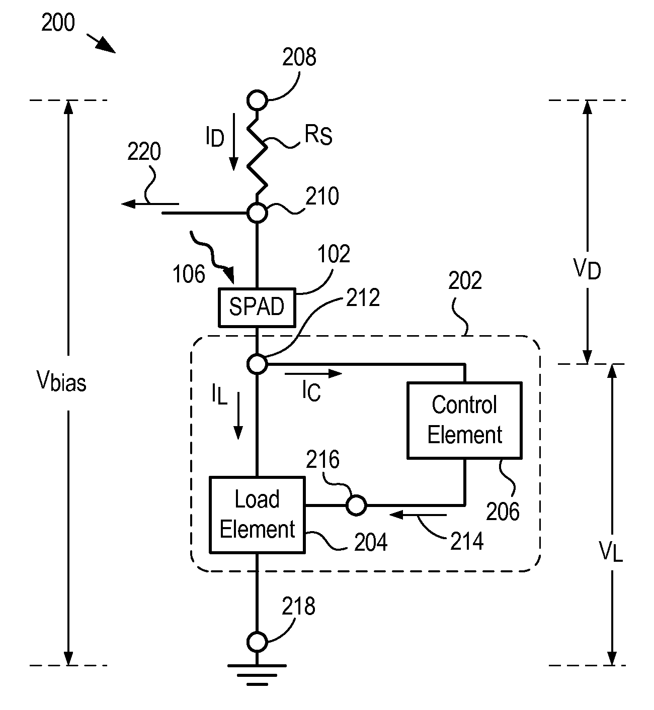
[0026]The following terms are defined for use in this Specification, including the appended claims:[0027]Single-photon avalanche diode (SPAD) is defined as an avalanche photodiode structure designed and intended for operation in Geiger mode.[0028]Negative feedback avalanche diode (NFAD) is defined as a SPAD that is operatively coupled with a negative feedback load. Preferably, the negative feedback load and SPAD are monolithically integrated.[0029]Electrically connected is defined as being in direct electrical contact. Two terminals are considered electrically connected if each remains at the same voltage potential for substantially any magnitude of electrical current through them (neglecting any inadvertent voltage drop through a conductive electrical line or trace used to connect the terminals together).

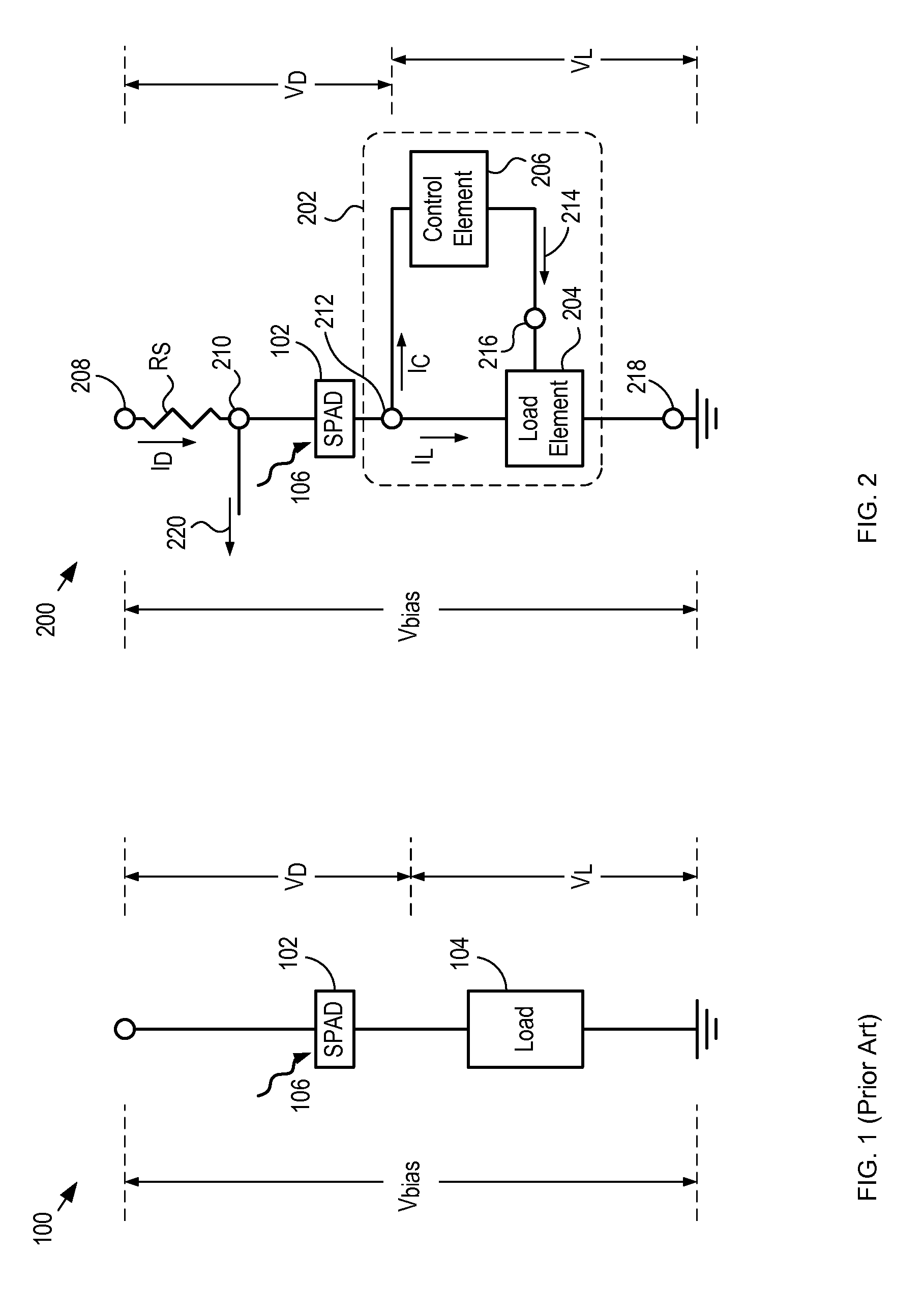
[0030]FIG. 1 depicts a schematic drawing of an NFAD in accordance with the prior art. NFAD 100 comprises SPAD 102 and load 104.

[0031]SPAD 102 is an avalanche photodiode that is dim...


PUM


Abstract

A negative feedback avalanche diode for detecting the receipt of a single photon is described. The photodetector comprises a load element having two load states, one characterized by high impedance and the other characterized by low impedance. The load state of the load element is controlled by a control signal generated within the negative feedback avalanche diode itself.

Description

CROSS-REFERENCE TO RELATED APPLICATION[0001]This application claims the benefit of U.S. provisional application Ser. No. 61 / 577,227, filed 19 Dec. 2011, entitled “Two-state Negative Feedback Avalanche Diode,” which is incorporated by reference.STATEMENT REGARDING FEDERALLY SPONSORED RESEARCH[0002]This invention was made with Government support under W31P4Q10C0164 awarded by the Defense Advanced Research Projects Agency (DARPA). The Government has certain rights in the invention.FIELD OF THE INVENTION[0003]The present invention relates to avalanche photodetectors in general, and, more particularly, to single-photon avalanche photodetectors.BACKGROUND OF THE INVENTION[0004]Photodetectors capable of detecting a single photon (i.e., a single “particle” of optical energy) are useful in many applications. To date, most of these applications have relied on the use of single-photon detectors such as photomultiplier tubes (PMTs) or single-photon avalanche detectors (SPADs) that are silicon-b...

Claims


Application Information

Patent Timeline
Patent Type & Authority Patents(United States)
IPC IPC(8): H01J40/14H03K17/78
CPCH03K17/78H01L31/02027H04N25/773
Inventor JIANG, XUDONGITZLER, MARK ALLENPATEL, KETAN MUKUND
Owner LG INNOTEK CO LTD
Why Eureka
Try Eureka