Method of fabricating substrate for organic light-emitting device

a technology of organic light-emitting devices and substrates, which is applied in the field of substrates for organic light-emitting devices, can solve the problems of reducing the longevity of the device, the inability to commercially use this technique, and the large increase in the cost of fabricating, so as to improve the light extraction efficiency, increase the light extraction efficiency of the organic light-emitting device, and achieve the effect of improving the transmittance of the substra

Inactive Publication Date: 2015-05-19
SAMSUNG CORNING PRECISION MATERIALS CO LTD
View PDF2 Cites 0 Cited by
  • Summary
  • Abstract
  • Description
  • Claims
  • Application Information

AI Technical Summary

Benefits of technology

[0013]Various aspects of the present invention provide a substrate for an organic light-emitting device or a substrate which can improve the light extraction efficiency of an organic light-emitting device while realizing an intended level of transmittance, a method of fabricating the same, and an organic light-emitting device having the same.
[0024]According to embodiments of the present invention, it is possible to control the refractive index of the substrate and the size of crystallized particles inside the substrate through heat treatment to the substrate. Since light generated from the OLED is scattered through the crystallized particles inside the substrate while passing through the substrate, the light extraction efficiency of the organic light-emitting device is increased and the transmittance of the substrate can be realized.
[0025]In addition, it is possible to improve the light extraction efficiency by increasing the transmission of light that propagates straight by arranging the crystallized particles into a specific pattern.
[0026]Furthermore, since the substrate made of transparent crystallization glass having a high surface flatness serves not only as an external light extraction layer but also as an internal light extraction layer of an organic light-emitting device, it is possible to further simplify the structure over a conventional organic light-emitting device in which an external light extraction layer and an internal light extraction layer are formed on both surfaces of a glass substrate. Accordingly, it is possible to realize structural firmness and preclude the external and internal light extraction layers and the planarization film that would otherwise be provided separate from the glass substrate, thereby simplifying the fabrication process and reducing the fabrication cost.
[0027]In addition, when the substrate made of transparent crystallization glass is applied for a light extraction substrate of an organic light-emitting device, it is possible to reduce power consumption of the organic light-emitting device through the improved light extraction efficiency of the organic light-emitting device. This can consequently minimize heat generation, thereby increasing the longevity of the organic light-emitting device.

Problems solved by technology

However, silica aerogel is very sensitive to moisture and is unstable, thereby resulting in the reduced longevity of the device.
Accordingly, it was impossible to commercially use this technique.
In addition, although the technique of using the micro-lenses or mesa structure increased the external light efficiency, the fabricating cost was greatly increased.
This consequently causes the problem of low practicability.
However, since glass is amorphous, it is very difficult to form the texture structure having a certain shape on the glass plate.
Consequently, the texture structure is also formed on the surface of the anode that adjoins to the glass plate, whereby leakage current occurs.
This consequently creates many problems in the structure or process.

Method used


Image

  • Method of fabricating substrate for organic light-emitting device
  • Method of fabricating substrate for organic light-emitting device
  • Method of fabricating substrate for organic light-emitting device

Examples


Embodiment Construction

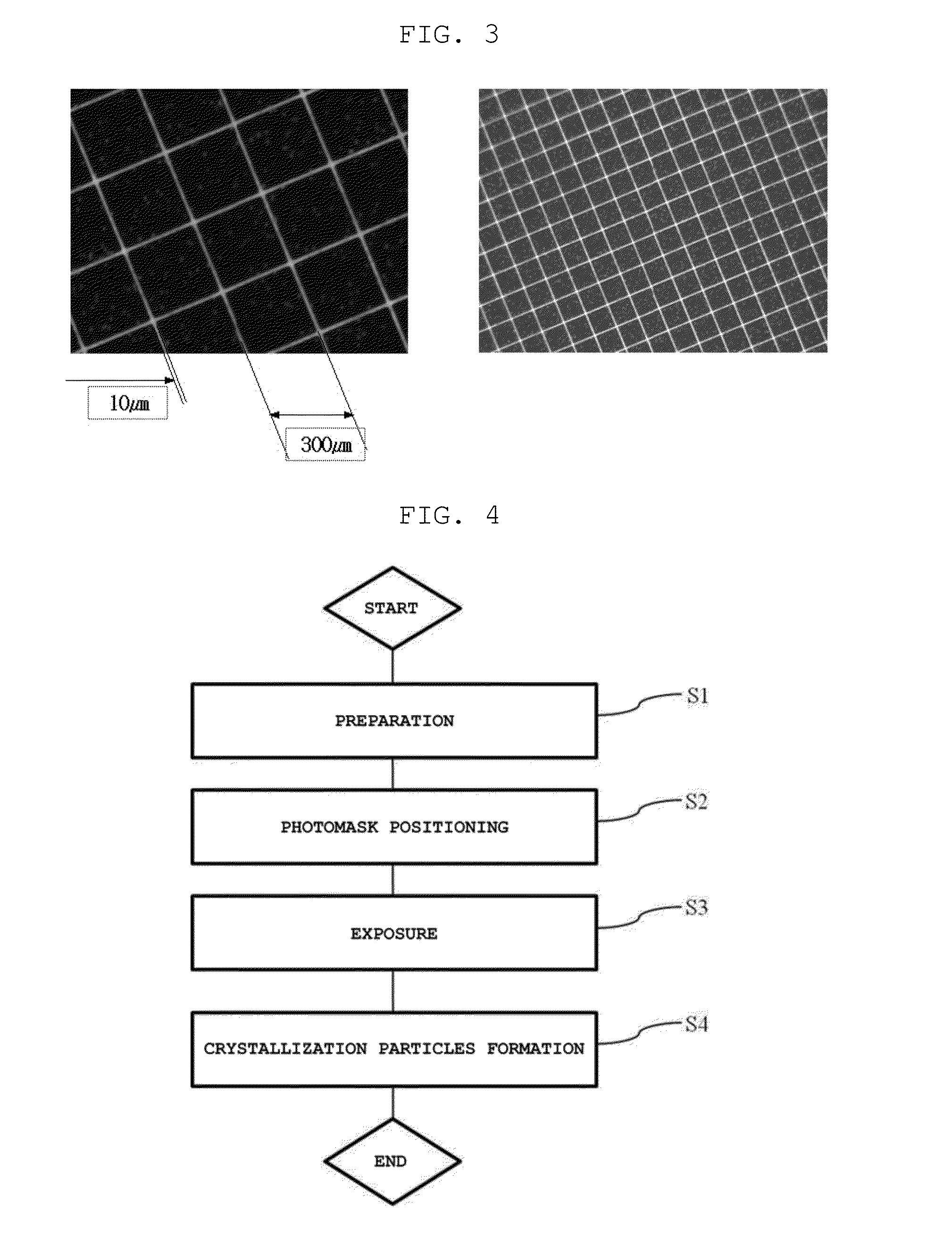
[0035]Reference will now be made in detail to a substrate, a method of fabricating the same, and an organic light-emitting device having the same according to the present invention, embodiments of which are illustrated in the accompanying drawings and described below, so that a person skilled in the art to which the present invention relates can easily put the present invention into practice.

[0036]Throughout this document, reference should be made to the drawings, in which the same reference numerals and signs are used throughout the different drawings to designate the same or similar components. In the following description of the present invention, detailed descriptions of known functions and components incorporated herein will be omitted when they may make the subject matter of the present invention unclear.

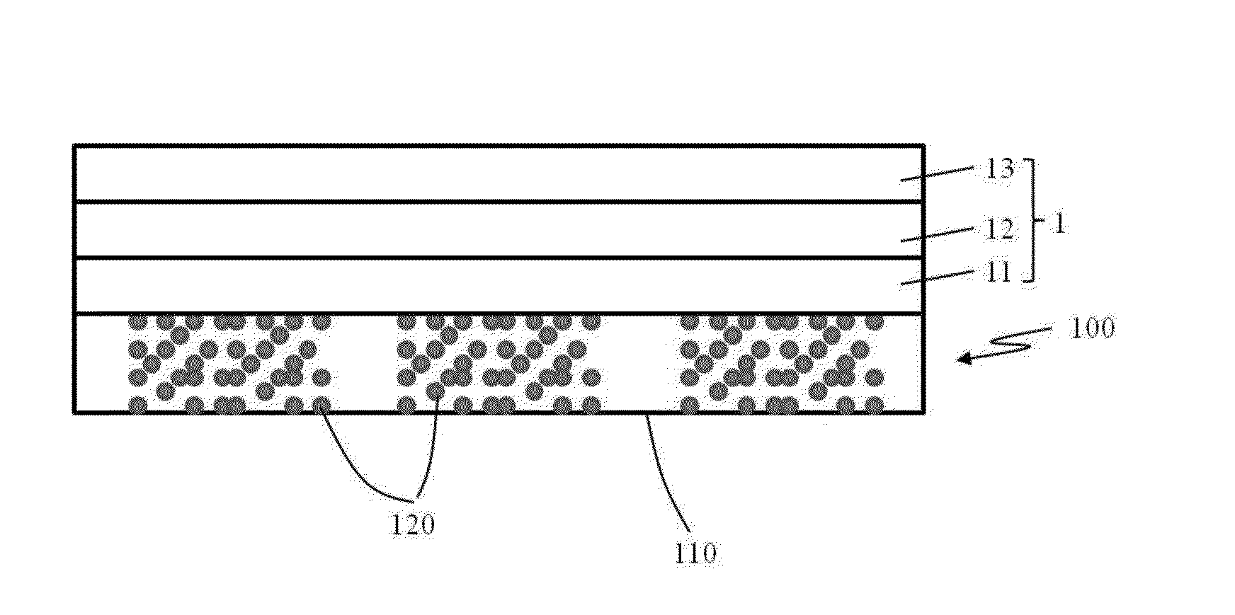
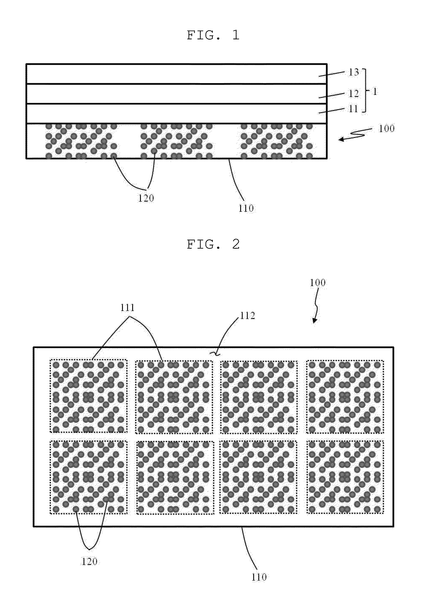
[0037]As shown in FIG. 1 and FIG. 2, a substrate 100 according to an exemplary embodiment of the invention is one of a pair of substrates of an organic light-emitting device w...


PUM

PropertyMeasurementUnit
particle sizeaaaaaaaaaa
refractive indexaaaaaaaaaa
visible transmittanceaaaaaaaaaa

Abstract

A substrate for an organic light-emitting device which can improve the light extraction efficiency of an organic light-emitting device while realizing an intended level of transmittance, a method of fabricating the same, and an organic light-emitting device having the same. Light emitted from the OLED is emitted outward through the substrate. The substrate includes a substrate body and a number of crystallized particles disposed inside the substrate body, the number of crystallized particles forming a pattern inside the substrate body.

Description

CROSS REFERENCE TO RELATED APPLICATION[0001]The present application claims priority from Korean Patent Application Number 10-2013-0050552 filed on May 6, 2013, the entire contents of which are incorporated herein for all purposes by this reference.BACKGROUND OF THE INVENTION[0002]1. Field of the Invention[0003]The present invention relates to a substrate for an organic light-emitting device, a method of fabricating the same, and an organic light-emitting device having the same, and more particularly, to a substrate which can improve the light extraction efficiency of an organic light-emitting device while realizing an intended level of transmittance, a method of fabricating the same, and an organic light-emitting device having the same.[0004]2. Description of Related Art[0005]In general, an organic light-emitting diode (OLED) includes an anode, a light-emitting layer and a cathode. When a voltage is applied between the anode and the cathode, holes are injected from the anode into a ...

Claims


Application Information

Patent Timeline
Patent Type & Authority Patents(United States)
IPC IPC(8): G03F7/26G03F7/004G03F7/40
CPCG03F7/40G03F7/0042Y02E10/549H10K71/00H10K77/10H10K50/80H10K2101/00
Inventor LEE, KIYEONKIM, JHEE-MANNLEE, YOUNGSEOKYOON, KYUNGMINLEE, JAEHO
Owner SAMSUNG CORNING PRECISION MATERIALS CO LTD
Why Eureka
Try Eureka