
Large area organic light emitting diode display and method for manufacturing the same

a technology of organic light emitting diodes and large area, which is applied in the direction of basic electric elements, electrical equipment, semiconductor devices, etc., can solve the problems of not developing the mass manufacturing method of large area display having the 20 inch or more diagonal area such as tv monitors, and is difficult to pattern organic light emitting materials using the currently used photo lithography method, etc., to achieve reliable and stable production yield, high resolution

Active Publication Date: 2015-06-09
LG DISPLAY CO LTD
View PDF1 Cites 23 Cited by
  • Summary
  • Abstract
  • Description
  • Claims
  • Application Information

AI Technical Summary

Benefits of technology

The present patent aims to provide a method for manufacturing a large area organic light emitting diode display without any damages on the organic light emitting layer. This method can use the photo lithography process to pattern the organic light emitting layer and electron transport layer simultaneously, resulting in a stable pattern over a large area. Additionally, this method can produce high resolution displays with reliable and stable production yield. Overall, the present patent offers a solution to overcome the limitations of current manufacturing methods and provide greater flexibility and efficiency for organic light emitting diode displays.

Problems solved by technology

However, the mass manufacturing method for large area display having the 20 inch or more diagonal area such as TV monitor has not been developed.
However, it is very hard to pattern the organic light emitting material by the currently used photo lithography method, while ensuring a stable and reliable pattern quality.
However, when the display size is larger than 20 inches, it is almost impossible to form the organic light emitting layer within specified areas over a large area using the screen mask process.
This is because as the size of the display area increases, the size and weight of the screen mask also increases.
The additional size and weight of the screen mask causes the screen mask to sag in the middle so that it becomes non-planar.
As a result, it is hard to deposit the organic light emitting material with uniform thickness over the large area substrate with a screen mask.
Furthermore, in order to accomplish a mass production method for manufacturing the large area organic light emitting diode display, there are many problems to be overcome.

Method used


Image

  • Large area organic light emitting diode display and method for manufacturing the same
  • Large area organic light emitting diode display and method for manufacturing the same
  • Large area organic light emitting diode display and method for manufacturing the same

Examples


second embodiment

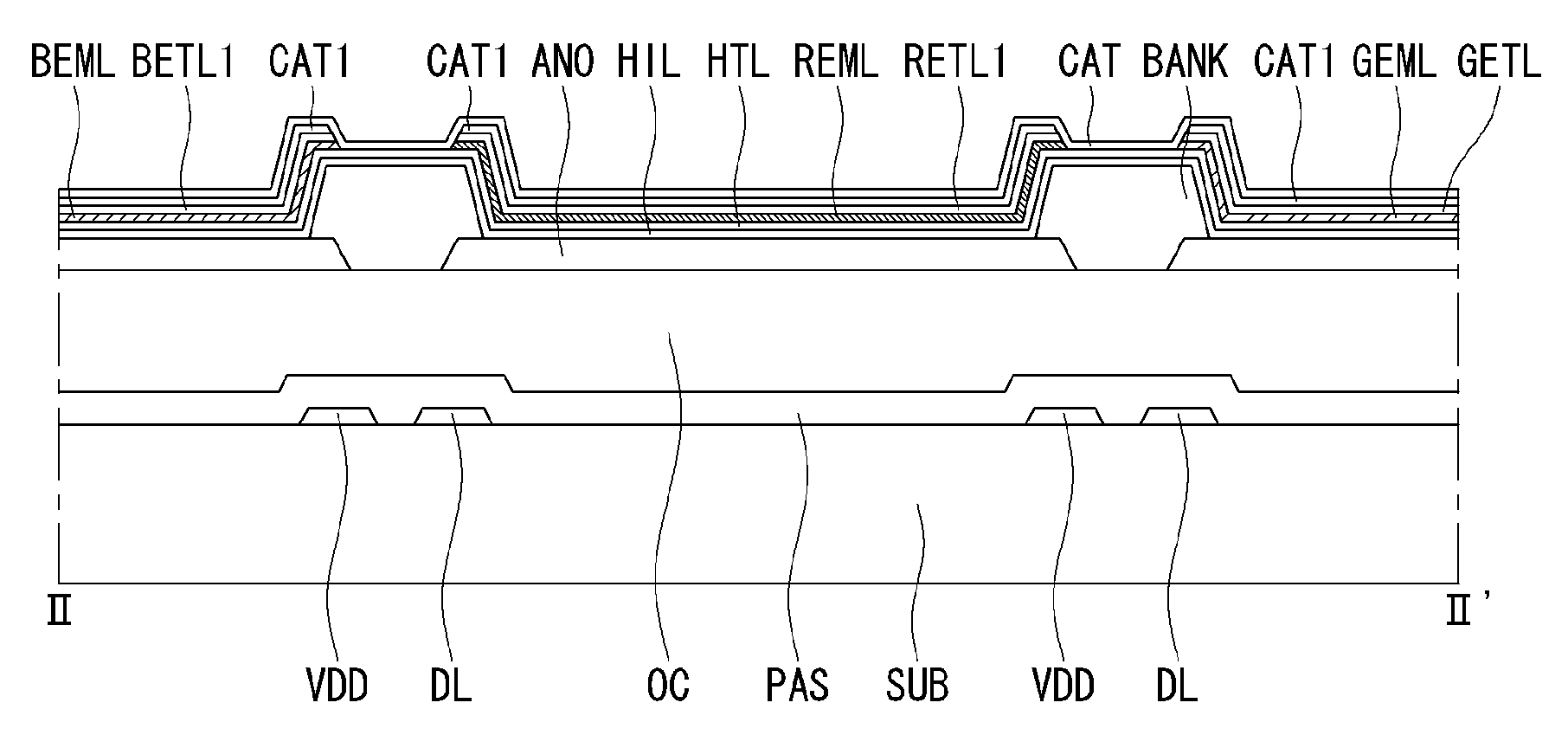
[0070]Referring to FIG. 8, we will explain a large area organic light emitting diode display according to the present disclosure. A hole injection layer HIL is deposited on the anode electrode ANO and the bank BANK, over the whole surface of the substrate SUB. A hole transport layer HTL is deposited on the hole injection layer HIL over the whole surface of the substrate SUB. As the hole injection layer HIL and the hole transport layer HTL cover the whole surface of the substrate SUB, a photo mask process or screen mask process is not required.

[0071]In each pixel area, any one of the red organic emission layer REML, the green organic emission layer GEML and the blue organic emission layer BEML is formed between the banks BANK on the hole transport layer HTL. Actually, the organic emission layers REML, GEML and BEML define their respective emitting areas. Therefore, it is preferred for the organic light emitting layers to cover the emitting area between adjacent banks BANK.

[0072]Furth...

third embodiment

[0074]Now, referring to FIG. 9, we will explain a large area organic light emitting diode display according to the present disclosure. A hole injection layer HIL is deposited on the anode electrode ANO and the bank BANK, and covers the whole surface of the substrate SUB. On the hole injection layer HIL, a hole transport layer HTL is deposited covering the whole surface of the substrate SUB. As the hole injection layer HIL and the hole transport layer HTL cover the whole surface of the substrate SUB, a photo mask process or screen mask process is not required.

[0075]In each pixel area, any one of the red organic emission layer REML, the green organic emission layer GEML and the blue organic emission layer BEML is formed between the banks BANK on the hole transport layer HTL. Additionally, the emitting area is defined by the organic emission layers REML, GEML and BEML. Therefore, it is preferable for the organic light emitting layers to cover the emitting area between adjacent banks BA...


PUM


Abstract

The present disclosure relates to a large area organic light emitting diode display and a method for manufacturing the same. A photoresist is deposited across first and second pixel areas of the display. The photoresist is patterned to generate a patterned photoresist by stripping away first portions of the photoresist in the first pixel areas while keeping second portions of the photoresist in the second pixel areas. An organic emission layer is deposited across the first and second pixel areas over the patterned photoresist. An electron transport layer is deposited across the first pixel areas and the second pixel areas over the organic emission layer. Portions of the organic emission layer and the electron transport layer in the second pixel areas are removed by stripping away the second portions of the photoresist while keeping portions of the organic emission layer and the electron transport layer in the first pixel areas.

Description

CROSS-REFERENCE TO RELATED APPLICATIONS[0001]This application claims the benefit of Korea Patent Application No. 10-2012-0151437 filed on Dec. 21, 2012, which is incorporated herein by reference for all purposes as if fully set forth herein.BACKGROUND[0002]1. Field of the Invention[0003]The present disclosure relates to a large area organic light emitting diode display and a method for manufacturing the same. Especially, the present disclosure relates to a large area organic light emitting diode display having color light emitting diode in each pixel and a method for manufacturing the same with a photo lithography process.[0004]2. Discussion of the Related Art[0005]Nowadays, various flat panel display devices are developed for overcoming many drawbacks of the cathode ray tube such as heavy weight and bulk volume. The flat panel display devices include the liquid crystal display device (or LCD), the field emission display (or FED), the plasma display panel (or PDP) and the electrolum...

Claims


Application Information

Patent Timeline
Patent Type & Authority Patents(United States)
IPC IPC(8): H01L51/56H01L51/52H01L29/08
CPCH01L51/56H01L51/52H01L29/08H10K71/00H10K59/353H10K59/121H10K50/16H10K50/80H10K50/11H10K50/17
Inventor KIM, YOUNGMIHEO, JOONYOUNGLEE, YEONKYEONGPARK, YONGMIN
Owner LG DISPLAY CO LTD
Learn More