Semiconductor laser device, semiconductor laser module, and raman amplifier using the device or module

a laser device and semiconductor technology, applied in the direction of lasers, lasers, optical resonator shapes and constructions, etc., can solve the problems of inability to carry out stable raman amplification, limited application excitation methods, and increase in costs, and achieve stable output and high efficiency

Active Publication Date: 2005-01-27
FURUKAWA ELECTRIC CO LTD
View PDF3 Cites 10 Cited by
  • Summary
  • Abstract
  • Description
  • Claims
  • Application Information

AI Technical Summary

Benefits of technology

It is an object of the present invention to provide a semiconductor laser device that is suitable for excitation light source for a Raman amplifier or the like, and t...

Problems solved by technology

Therefore, there has been a problem of increase in cost along the increase in the transmission capacity.
The fluctuation of the Raman gain is directly output as the fluctuation of the amplified signal intensity, which causes a problem in that stable Raman amplification cannot be carried out.
The reason is that the front-side excitation method in which the weak signal light proceeds in the same direction together with the strong exciting light has a problem in that the exciting light intensity...

Method used


Image

  • Semiconductor laser device, semiconductor laser module, and raman amplifier using the device or module
  • Semiconductor laser device, semiconductor laser module, and raman amplifier using the device or module
  • Semiconductor laser device, semiconductor laser module, and raman amplifier using the device or module

Examples


first embodiment

(First Embodiment)

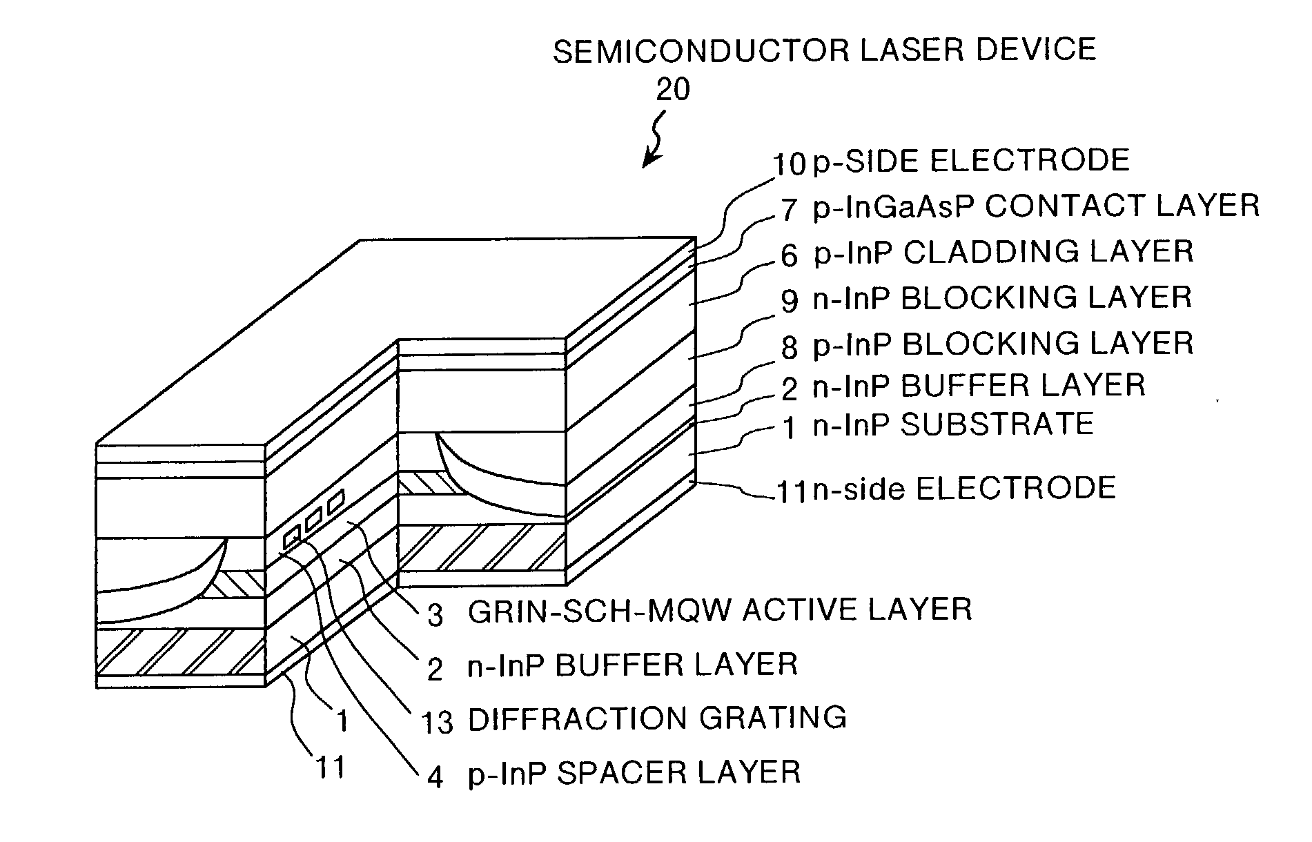
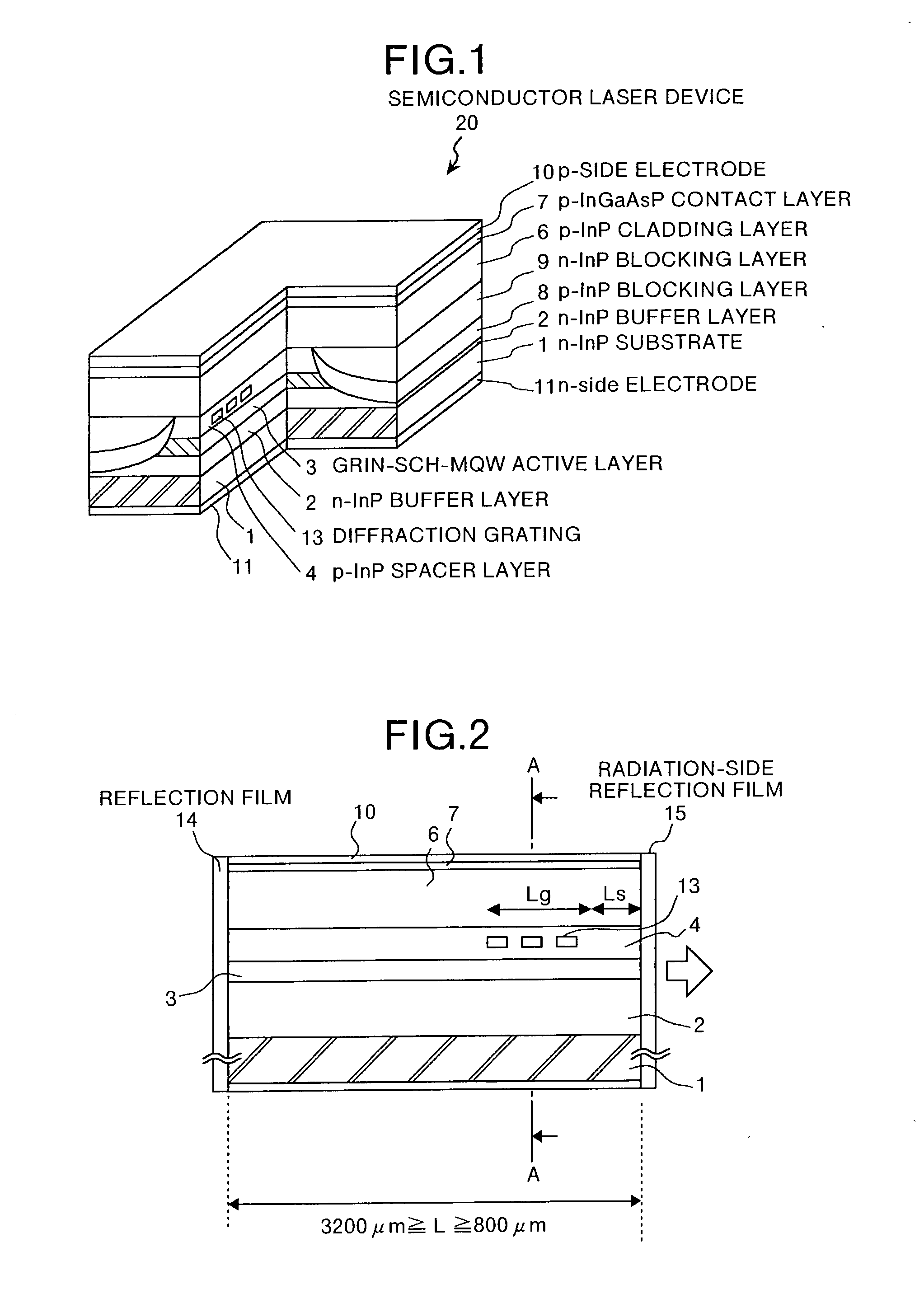
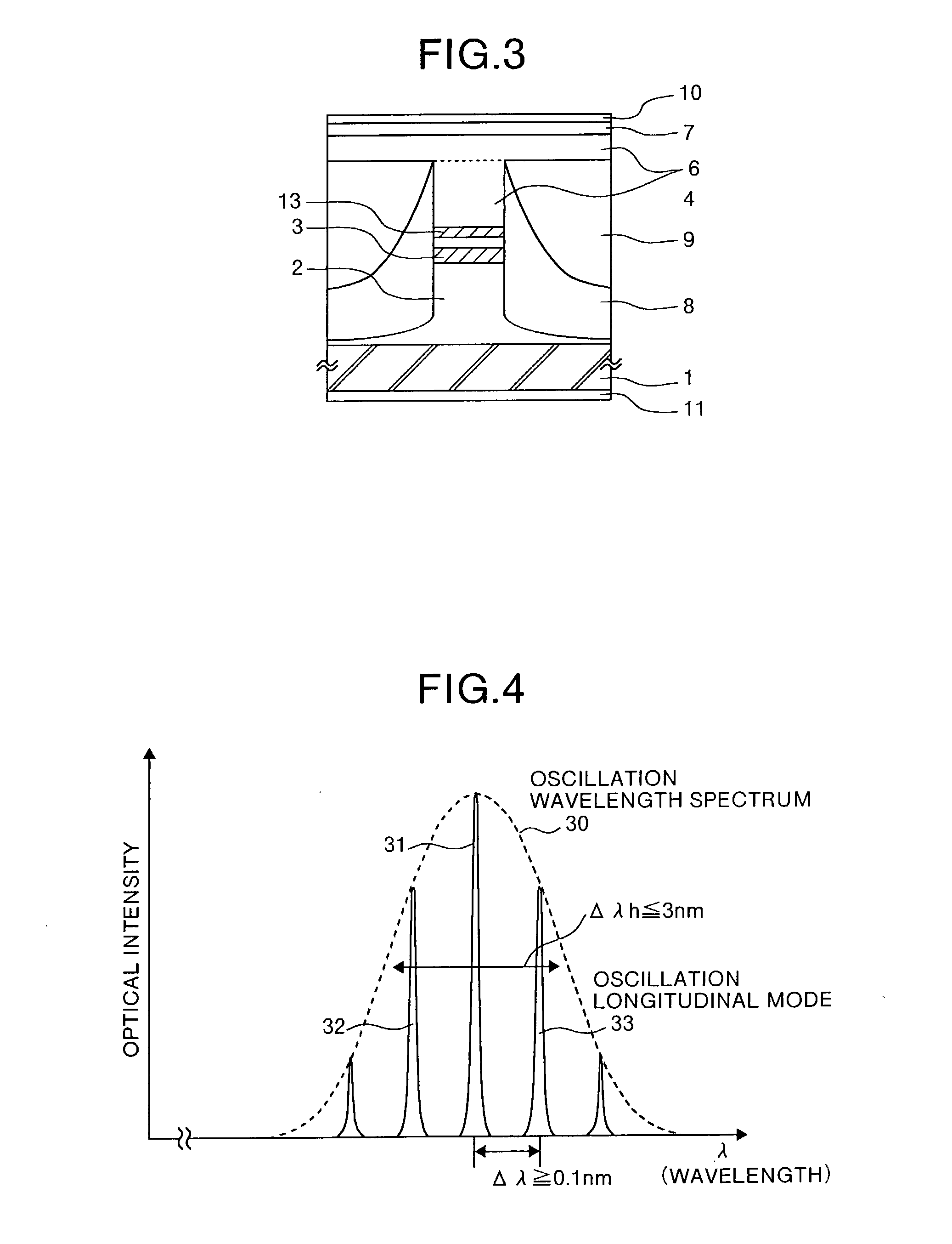
First, a first embodiment of the present invention will be, explained. FIG. 1 is a cutaway view of a semiconductor laser device according to a first embodiment of the present invention as viewed from a slanting direction. FIG. 2 is a longitudinal sectional view in a longitudinal direction of the semiconductor laser device shown in FIG. 1. FIG. 3 is a cross-sectional view of the semiconductor laser device shown in FIG. 2 taken along the line A-A. In FIGS. 1 to 3, a semiconductor laser device 20 has a structure in which on a plane (100) of an n-InP substrate 1, the following elements are sequentially laminated; an n-InP cladding layer 2 serving as a buffer layer and a lower cladding layer by an n-InP, a GRIN-SCH-MQW (Graded Index-Separate Confinement Heterostructure Multi Quantum Well) active layer 3 having compressive strain, a P-InP spacer layer 4, a p-InP cladding layer 6 and an InGaAsP contact layer 7.

The P-InP spacer layer 4 is provided therein with a diffrac...

second embodiment

(Second Embodiment)

A second embodiment of the invention will now be explained. In the second embodiment, the semiconductor laser device shown in the above-described first embodiment is modularized.

FIG. 14 is a longitudinal sectional view that shows a structure of a semiconductor laser module of the second embodiment of the invention. In FIG. 14, a semiconductor laser module 50 includes a semiconductor laser device 51 corresponding to the semiconductor laser device shown in the above-described first to third embodiments. The semiconductor laser device 51 is of a junction-down structure in which a p-side electrode is connected to a heat sink 57a. A Peltier element 58 as a temperature control device is disposed on a bottom surface inside a package 59 formed of ceramic as a housing of the semiconductor laser module 50. A base 57 is disposed on the Peltier element 58, and the heat sink 57a is disposed on the base 57. Current (not shown) is supplied to the Peltier element 58, and coolin...

third embodiment

(Third Embodiment)

Next, a third embodiment of the present invention will be explained. In the third embodiment, the semiconductor laser module shown in the second embodiment is applied to the Raman amplifier.

FIG. 15 is a block diagram that shows a structure of a Raman amplifier of the third embodiment of the invention. The Raman amplifier is used for the WDM communication system. In FIG. 15, the Raman amplifier uses semiconductor laser modules 60a to 60d having the same structure as that of the semiconductor laser module shown in the second embodiment, and it is of a structure such that semiconductor laser modules 182a to 182d shown in FIG. 22 are replaced by the above-described semiconductor laser modules 60a to 60d.

Each of the semiconductor laser modules 60a and 60b outputs a laser beam having a plurality of oscillation longitudinal modes to the polarization beam combiner 61a through a polarization maintaining fiber 71. Each of the semiconductor laser modules 60c and 60d outpu...


PUM


Abstract

A semiconductor laser device which has a diffraction grating partially provided in the vicinity of an active layer formed between a radiation-side reflection film provided on a radiation-side end surface of a laser beam and a reflection film provided on a reflection-side end surface of the laser beam, and which outputs a laser beam having a desired oscillation longitudinal mode based on a wavelength selection characteristic of at least the diffraction grating. The diffraction grating is formed in isolation with an isolation distance of Ls=15 μm from the radiation-side reflection film.

Description

FIELD OF THE INVENTION The present invention relates to a semiconductor laser device suitable for application to an excitation light source such as a Raman amplifier, a semiconductor laser module and a Raman amplifier using the device or the module. BACKGROUND OF THE INVENTION In recent years, along the distribution of various multimedia such as Internet, there has been an increasing demand for the increase in the capacity of optical communications. Conventionally, in the optical communications, it has been general to transmit information using a single wavelength in a band of 1310 nm or 1550 nm as a wavelength that has small light absorption by an optical fiber. In this method, it is necessary to increase the number of cores of optical fibers that are laid in a transmission path in order to transmit a large quantity of information. Therefore, there has been a problem of increase in cost along the increase in the transmission capacity. Therefore, a DWDM (Dense-Wavelength Division...

Claims


Application Information

Patent Timeline
IPC IPC(8): H01S3/08H01S3/30H01S5/00H01S5/125H01S5/16
CPCH01S3/06754H01S3/094073H01S3/094096H01S3/302H01S5/02284H01S2301/16H01S5/06258H01S5/1215H01S5/125H01S5/146H01S5/16H01S5/02415H01S5/02251
Inventor YOSHIDA, JUNJITSUKIJI, NAOKIIRINO, SATOSHI
Owner FURUKAWA ELECTRIC CO LTD
Why Eureka
Try Eureka