
Wideband active balun LNA topology with narrow-band filtering and noise cancelling

a wideband active balun and wideband filtering technology, applied in the field of communication systems, can solve the problems of limiting the overall linearity and noise performance, poor iip2 performance of such a structure, and the inability to achieve low noise and impedance matching simultaneously, so as to achieve balanced differential signal output, improve linearity performance and noise performance of the entire circuit, and improve the effect of iip2 performan

Active Publication Date: 2015-06-09
MONTAGE TECHNOLOGY CO LTD
View PDF1 Cites 41 Cited by
  • Summary
  • Abstract
  • Description
  • Claims
  • Application Information

AI Technical Summary

Benefits of technology

The present invention introduces a new topology for a wideband active balun LNA which debuts with a noise cancelling feature. This results in improved linearity and reduced noise in a compact design without the need for additional stages. Additionally, the invention enables single-to-differential conversion with a balanced differential signal output and suppressed second-order intermodulation, leading to superior performance. Furthermore, by canceling out noise from transistors used for impedance matching, the invention achieves low noise performance.

Problems solved by technology

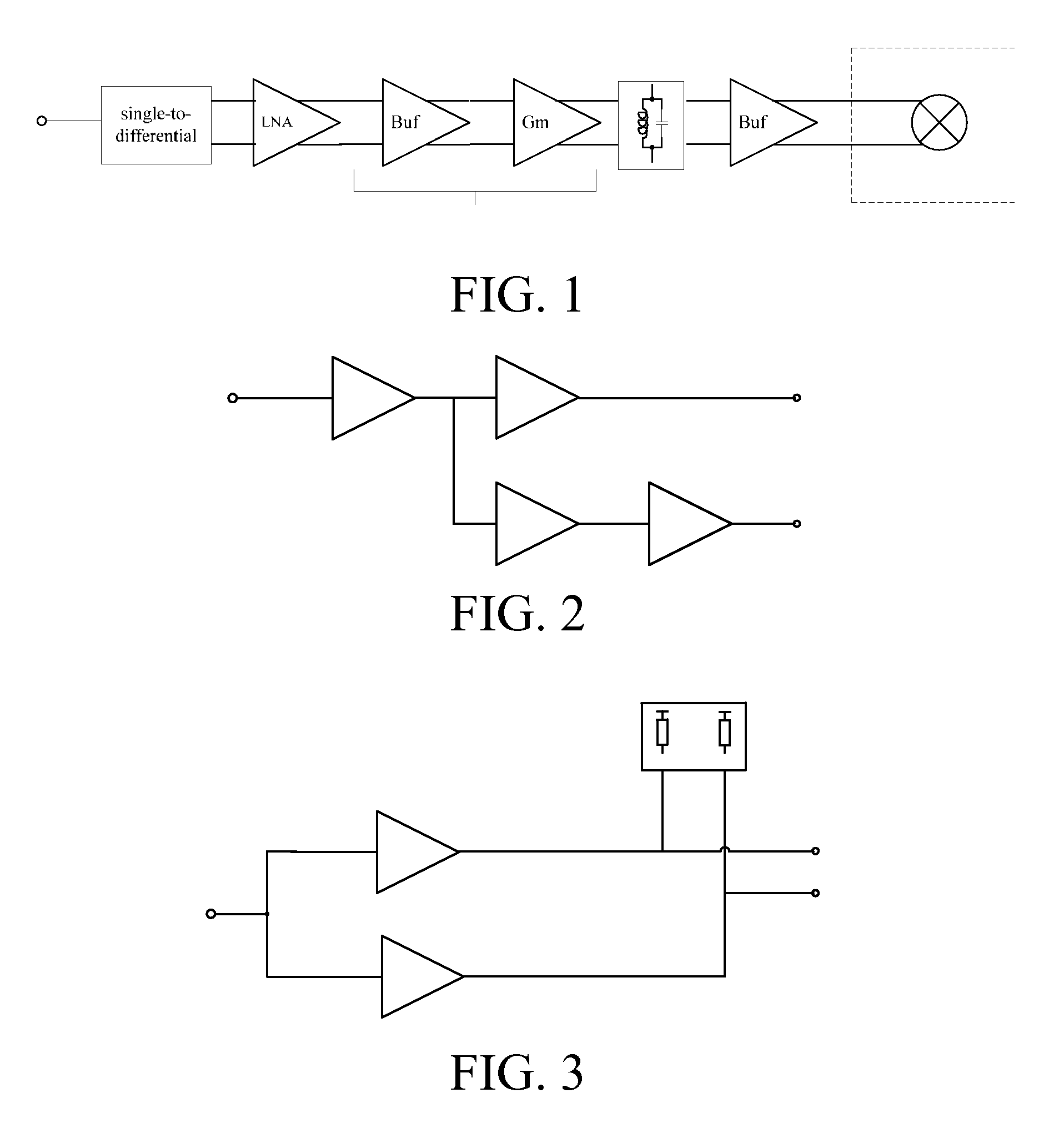
The buffer stage and the transconductance (Gm) stage that serve as interface stages consume a substantial sum of power and use more chip-area and also limit the overall linearity and noise performance.
The disadvantage of such structure is that it is impossible to achieve low noise and impedance matching simultaneously.
However, the disadvantage of such a structure is poor IIP2.
However, this structure has some drawbacks as follows: a current mirror limits the bandwidth of the circuit and the current mirror itself introduces much noise whereas second-order linearity basically depends on the matching between PMOS and NMOS, which can result in a relatively sensitive IIP2.
The wideband low-noise amplifier structures introduced above are capable of implementing a relatively low noise figure, however, they can't satisfy the requirement of single-to-differential conversion on a chip, and it is difficult for them to attain good second-order linearity either.
However, only a small number of LNA structures can obtain single-to-differential conversion in a wide bandwidth.
Therefore, a load filter circuit similar to LC Tank cannot be directly connected to the output thereof.
In view of implementing filtering, a stage such as transconductance stage (Gm) or buffer stage must be inserted between the LNA and the filter load (similar to the foregoing traditional approach), which simultaneously degrades noise performance and linearity performance, thereby further adding extra power consumption.
Although the structure can implement single-to-differential conversion on a chip, a filter circuit is placed at an RF input since it can't be implemented at output, resulting in a very narrow input matching bandwidth.
In addition, the noise figure of the entire circuit is relatively high without using noise cancellation technology.
The disadvantage is that the output impedance characteristic directly affects the input matching, thus failing to implement low-noise amplification and narrow-band filtering in one stage, if additional transconductance stage is inserted for filtering, the overall noise and linearity performance will be degraded.
The disadvantage of this structure is that: balanced differential output is implemented through a multi-stage DCB circuit, which is therefore constrained by both the voltage headroom of the circuit and the adjustability capability of the DCB circuit.
In addition, IIP2 performance of the circuit is still sensitive and is easily susceptible to the power supply, load, and performance of DCB circuit.
Although the structure can implement desirable IIP2 and NF, the unbalanced differential output makes it impossible for a load filter circuit similar to LC Tank to be implemented, unless an additional buffer stage or transconductance (Gm) stage is used.

Method used


Image

  • Wideband active balun LNA topology with narrow-band filtering and noise cancelling
  • Wideband active balun LNA topology with narrow-band filtering and noise cancelling
  • Wideband active balun LNA topology with narrow-band filtering and noise cancelling

Examples


embodiment

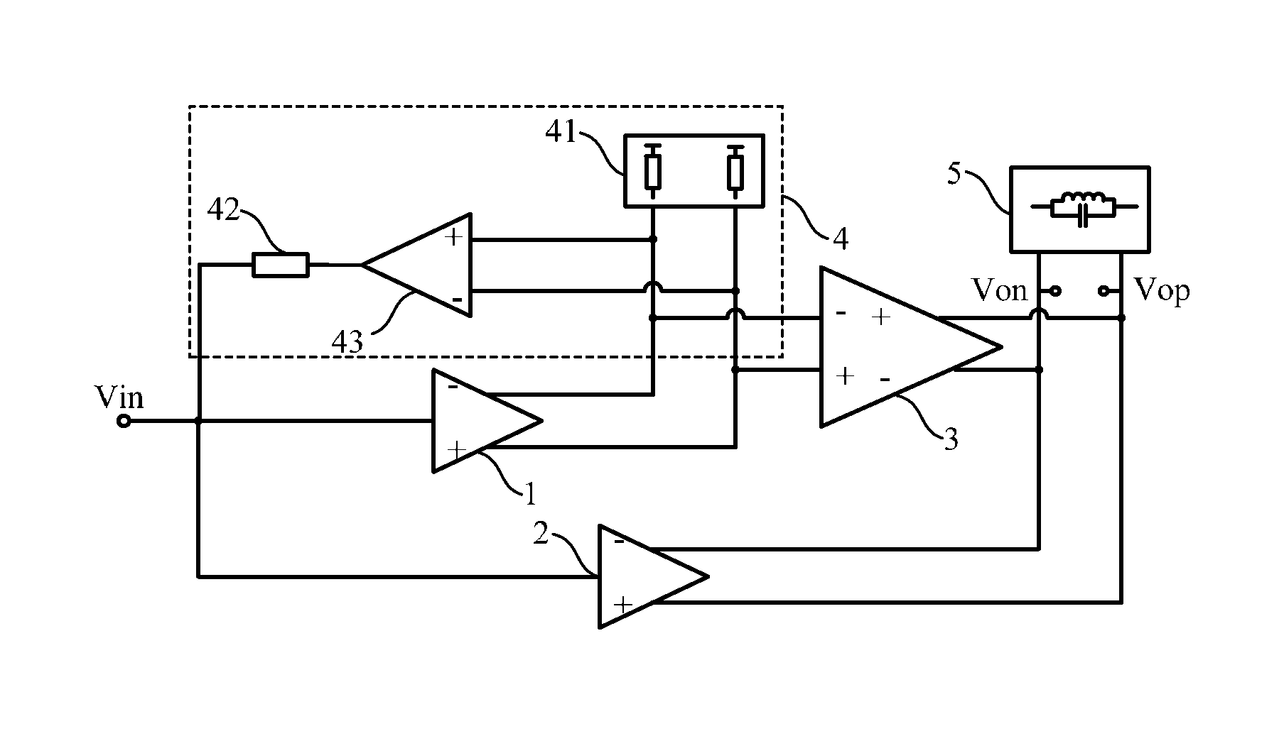
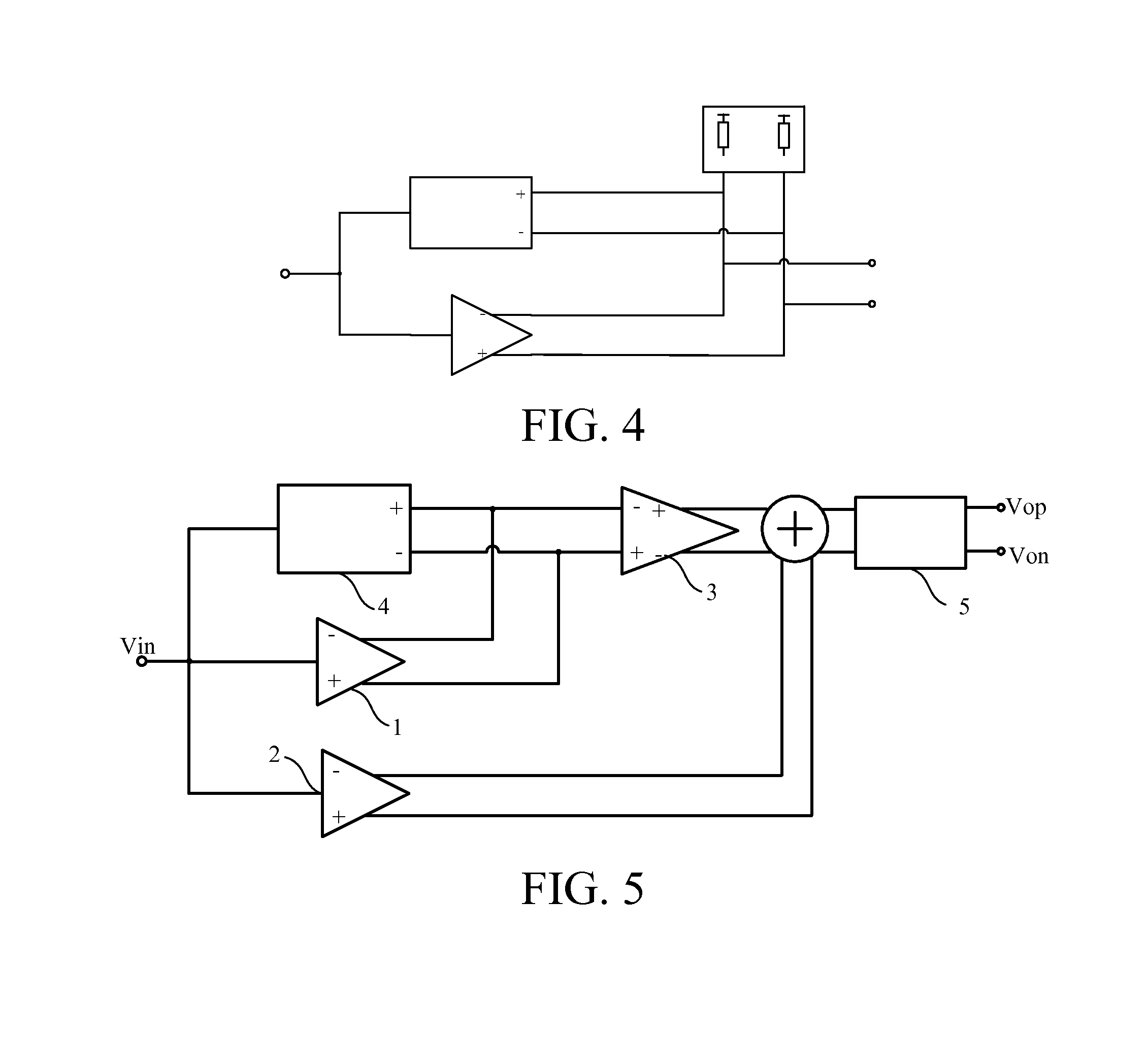
[0044]This embodiment provides a wideband active Balun low-noise amplifier topology. As shown in FIG. 5, the wideband low-noise amplifier topology includes: a first transconductance stage 1, a second transconductance stage 2, a third transconductance stage 3, a feedback network 4, and a load 5. As shown in FIG. 6, the feedback network 4 includes a load 41, a feedback resistor 42 (Rfb), and a feedback amplifier 43 (Amp-fb). The connection relationship inside the wideband low-noise amplifier topology is as follows: the first transconductance stage 1 and the second transconductance stage 2 are connected in parallel, a single-end input of the first transconductance stage 1 connects to a voltage input Vin, a first output (negative output) of the first transconductance stage 1 connects to a first input (negative input) of the third transconductance stage 3, a second output (positive output) of the first transconductance stage 1 connects to a second input (positive input) of the third tran...


PUM


Abstract

The present invention provides a wideband active balun LNA topology with narrow-band filtering and noise cancelling. The amplifier includes three transconductance stages, a feedback network, and a load. The first and second transconductance stages are connected in parallel to receive the input signal. The differential output of the first transconductance stage is fed back to voltage input through a differential-to-single-end-end feedback network, while the output of the first transconductance, passing through the third transconductance, is added to the output of the second transconductance stage in proper phase. The present invention accomplish both wideband low-noise amplification and narrow-band filtering without inserting interface stages, thereby improving the linearity and noise performance of the whole circuit. Noise cancellation technique is implemented in differential way to ensure the low noise figure. The present invention also achieves single-end to differential conversion with balanced output and superior second order linearity performance.

Description

BACKGROUND OF THE PRESENT INVENTION[0001]1. Field of Invention[0002]The present invention relates to the field of communication system, specifically to a low-noise amplifier (LNA), and more specifically to a wideband active balun LNA topology with narrow-band filtering and noise cancelling.[0003]2. Description of Related Arts[0004]Besides the basic requirements of low-noise amplification and impedance matching, the RF input front end of a wideband receiver is desired to be capable of handling tracking filtering and single-to-differential (S-to-D) conversion with stable second-order linearity and lower power consumption. In order to achieve such requirements, a general approach is as follows: RF signals passing through S-to-D network or LNA, and then being connected to a filter load through a buffer stage and a transconductance (Gm) stage to accomplish narrow-band tracking filtering, and then being connected to a mixer through the buffer stage. The buffer stage and the transconductan...

Claims


Application Information

Patent Timeline
IPC IPC(8): H03F1/26H03F3/19H03F3/45
CPCH03F1/26H03F3/19H03F3/45071H03F2003/45008H03F2200/451H03F2200/294H03F2200/372H03F2203/45051H03F1/42H03F3/195H03F3/211H03F3/45475H03F2203/45521H03F2203/45704
Inventor XU, JUN
Owner MONTAGE TECHNOLOGY CO LTD
Learn More