Method for manufacturing a hybrid integrated component

a technology of integrated components and manufacturing methods, applied in the direction of soldering devices, instruments, photomechanical devices, etc., can solve the problems of less space and less space on the application circuit boards of individual components, and achieve the effect of convenient and inexpensive permitting

Active Publication Date: 2015-06-30
ROBERT BOSCH GMBH
View PDF7 Cites 0 Cited by
  • Summary
  • Abstract
  • Description
  • Claims
  • Application Information

AI Technical Summary

Benefits of technology

[0008]Measures for the implementation of hybrid integrated components are proposed with the present invention, easily and inexpensively permitting an even higher degree of miniaturization.
[0011]The structure according to the present invention is suitable in particular for the implementation of contactless operating sensors, e.g., acceleration sensors, yaw rate sensors and other inertial sensors. In the case of an inertial sensor, the micromechanical sensor structure includes at least one elastically suspended seismic mass, which is deflected due to accelerations. These accelerations may also be induced by centrifugal forces or rotational movements. The deflections of the seismic mass are detected and evaluated. The micromechanical structure of such a sensor element should be capped to minimize environmental influences on the measuring signal and to protect the sensor structure from contaminants, moisture and particles. Defined pressure conditions for the sensor structure, which significantly codetermine the damping behavior of the sensor, may also be created in this way. Such capping or encapsulation is achieved according to the present invention by the sandwich configuration of the MEMS elements between the assigned ASIC elements without requiring separate cap structures.
[0013]As already mentioned, signal processing and evaluation circuits for the assigned MEMS elements are preferably integrated on the ASIC elements. However, the ASIC elements may of course also be furnished with other circuit functions. Furthermore, a structuring of the surface on which the MEMS substrate is to be mounted may also be carried out within the context of processing the ASIC substrates. Recesses in the ASIC surface as well as a pedestal structure for the mounting of the MEMS substrate may be provided. The mobility of structural elements in the assigned MEMS element, for example, may be ensured in this way.
[0017]With regard to a preferably compact structure of the component and reliable internal electrical contacting between the individual parts of the component, it has proven advantageous if through-contacts are created in at least one of the two MEMS substrates, establishing an electrical connection between the assigned ASIC substrate and the surface of the MEMS substrate facing away from this ASIC substrate.
[0018]As with the mounting of the MEMS substrates on the assigned ASIC substrates, the MEMS / ASIC wafer stacks are preferably also assembled in a bonding process since it is possible to easily establish reliable and durable mechanical and electrical connections between the two MEMS / ASIC wafer stacks in this way.

Problems solved by technology

Therefore, less and less space is available on the application circuit boards for the individual components.

Method used


Image

  • Method for manufacturing a hybrid integrated component
  • Method for manufacturing a hybrid integrated component
  • Method for manufacturing a hybrid integrated component

Examples


Embodiment Construction

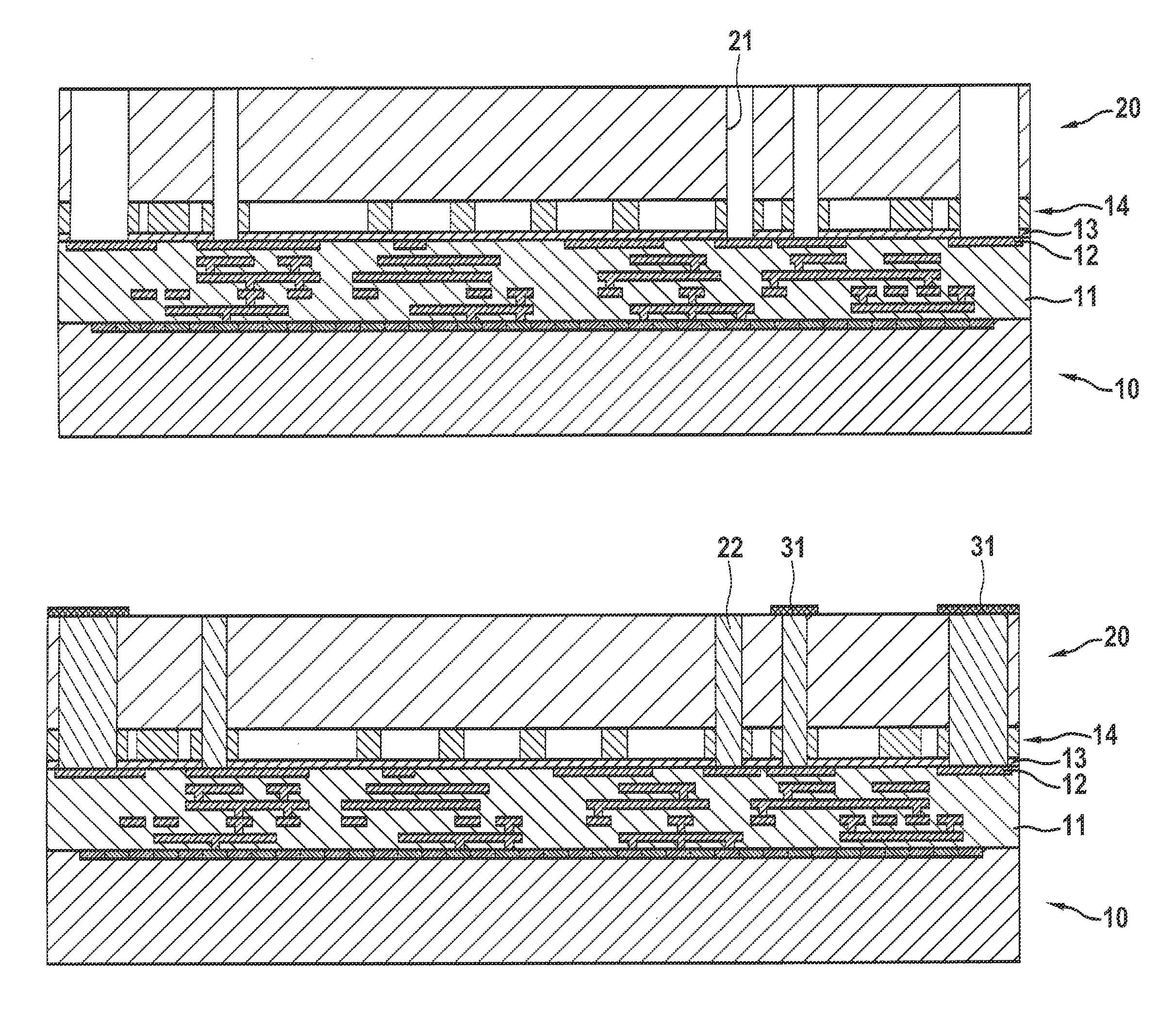
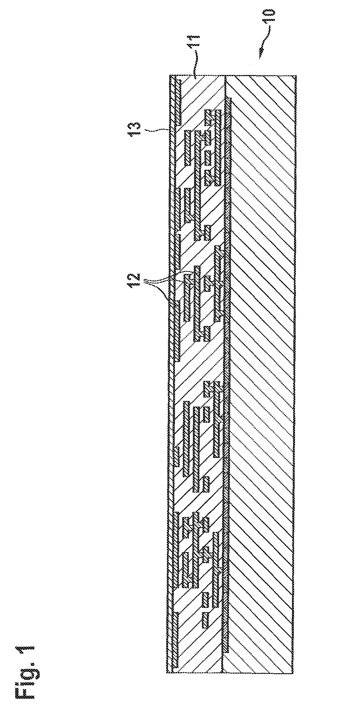
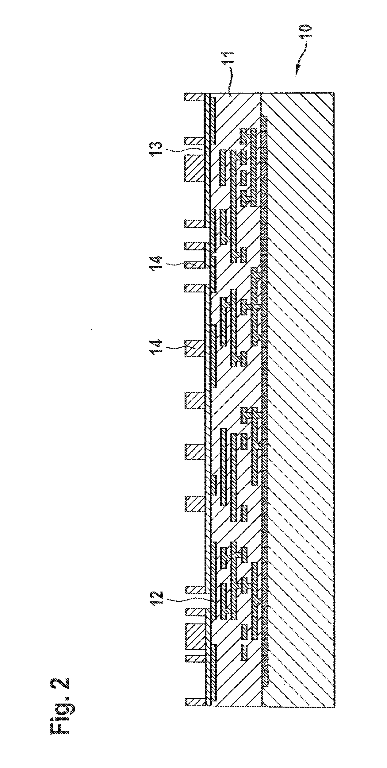
[0024]Within the context of the method according to the present invention for manufacturing a hybrid integrated component having two MEMS elements, at least one ASIC element being assigned to each, two MEMS / ASIC wafer stacks are initially created independently of one another. This is explained in greater detail below in conjunction with FIGS. 1 through 7.

[0025]The starting point for manufacturing such an MEMS / ASIC wafer stack is a processed ASIC substrate 10, as illustrated in FIG. 1. Multiple circuit levels 12 are formed in an oxide layer 11 on ASIC substrate 10. At least parts of a signal processing and evaluation circuit for the assigned MEMS element are advantageously integrated here. In addition, however, MEMS-independent circuit functions may also be implemented. The CMOS processing of ASIC substrate 10 is not described in detail here since it is not specified in detail by the present invention. The substrate surface is provided with a nitride passivation 13.

[0026]This passiva...


PUM

PropertyMeasurementUnit
aspect ratioaaaaaaaaaa
micromechanical structureaaaaaaaaaa
thicknessaaaaaaaaaa

Abstract

A manufacturing method for hybrid integrated components having a very high degree of miniaturization is provided, which hybrid integrated components each have at least two MEMS elements each having at least one assigned ASIC element. Two MEMS / ASIC wafer stacks are initially created independently of one another in that two ASIC substrates are processed independently of one another; a semiconductor substrate is mounted on the processed surface of each of the two ASIC substrates, and a micromechanical structure is subsequently created in each of the two semiconductor substrates. The two MEMS / ASIC wafer stacks are mounted on top of each other, MEMS on MEMS. Only subsequently are the components separated.

Description

BACKGROUND OF THE INVENTION[0001]1. Field of the Invention[0002]The present invention relates to a method for manufacturing a hybrid integrated component having at least two MEMS (microelectromechanical) system elements, at least one ASIC element being assigned to each.[0003]2. Description of the Related Art[0004]Components having MEMS elements have been manufactured in mass production for many years for greatly varying applications, for example, in the fields of automotive engineering and consumer electronics. The miniaturization of the components is increasingly gaining in significance. On the one hand, the miniaturization substantially contributes to reducing the manufacturing costs of the components and therefore also of the terminal equipment. On the other hand, in particular in the field of consumer electronics, more and more functions—and therefore components—are to be accommodated in the terminal equipment, while the terminal equipment itself becomes smaller and smaller. The...

Claims


Application Information

Patent Timeline
Patent Type & Authority Patents(United States)
IPC IPC(8): H01L21/30B81B7/00H01L29/84B81C3/00B81C1/00
CPCB81B7/008B81C3/001B81C1/00238B81C1/00246H01L2924/1433B81C2203/0771B81C2203/0735B81C2203/0785
Inventor CLASSEN, JOHANNESWEBER, HERIBERT
Owner ROBERT BOSCH GMBH
Why Eureka
Try Eureka